In the previous content of this packaging series, the author briefly introduced packaging processes such as RDL, TSV, and hybrid bonding. Next, the author plans to write two more articles about semiconductor packaging processes, which will briefly introduce the die attach process and underfill process, after which we will delve into the second major part of this packaging series, which is a detailed introduction to various packaging types.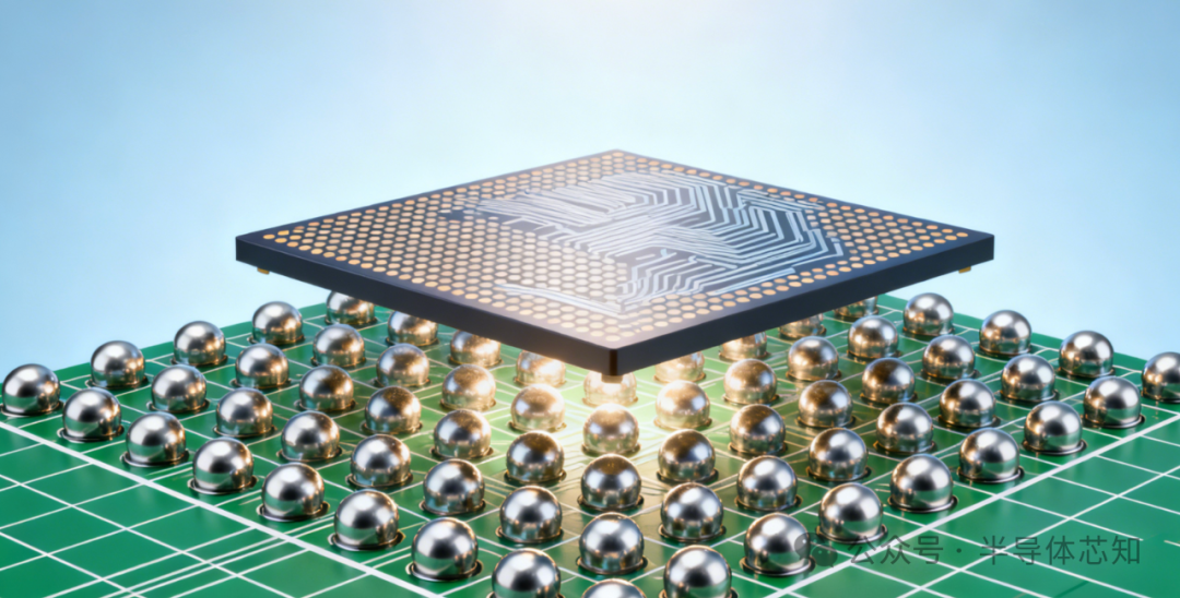 Below, the author has briefly organized the relevant content about die attach for your review.1. What is Die Attach?Die attach, or die bonding, is a process that we often hear about in various semiconductor popular science articles or videos, yet it is frequently glossed over. Therefore, the author would like to briefly explain what die attach is.Of course, as we understand, die attach is about fixing a bare chip to a package substrate or intermediary layer, which is correct. However, if you want to discuss this matter in detail, it is not that simple. Die attach is not just about securing the chip; it also involves establishing reliable thermal and electrical pathways, which relate to thermal resistance, void ratio, interface strength, and warpage. As chip sizes shrink, power levels increase, and packaging becomes more complex, the process window for die attach narrows sharply. A slight misstep can expose issues during subsequent bonding, RDL processes, or thermal cycling. For high-power devices such as AI chips, HBM, and SiC/GaN, a high thermal resistance or high void ratio at the attach interface can lead to frequent throttling or even failure. Therefore, the quality of die attach determines the thermal management capability and long-term reliability of the entire packaging system.2. Mainstream Die Attach Processes in the Industry: From Epoxy to Eutectic, to Silver SinteringCurrently, packaging factories commonly use three types of die attach technologies, each with distinctly different material systems and application scenarios.The most common is epoxy die attach, which uses silver paste or conductive adhesive to bond the chip to the substrate. This process is mature, cost-effective, and allows for flexible dispensing, making it the mainstream choice for consumer and mid-low power devices. However, its thermal conductivity is limited, and the curing process can easily introduce voids and stress, leading to its gradual replacement in high-power devices.Eutectic bonding resembles a form of micro-welding, forming a dense and reliable metal interface through Au-Sn, Au-Si, and other eutectic systems at specific temperatures. It offers higher thermal conductivity, fewer voids, and greater reliability, thus holding a firm position in high-end RF, automotive-grade chips, and some power devices. Its drawbacks include high material costs, narrow process windows, and stricter requirements for equipment and temperature profiles.What truly drives the revolution in semiconductor packaging is silver sintering, which achieves thermal conductivities far exceeding traditional materials by sintering silver powder or sheets into a dense metal layer under high-temperature conditions. It also features low voids, high reliability, and the ability to operate at high temperatures. As SiC and GaN become mainstream, silver sintering has almost become the default option, especially in scenarios where thermal management is critically sensitive, such as automotive, inverters, and server power supplies, where it has replaced solder and adhesives to become the “king of processes.” 3. Engineering Challenges of Die Attach: Voids, Warpage, and Interface ReliabilityRegardless of the technology route adopted, the core challenges of die attach consistently focus on three aspects. First is void control, which is the most challenging issue across all attachment technologies, as voids act as thermal insulators, directly increasing thermal resistance and reducing device lifespan. During dispensing, gas entrapment, and the inability to vent volatiles during curing, along with larger chip areas complicating venting, all contribute to increased void ratios. Therefore, the industry commonly relies on vacuum reflow soldering, low-volatile resin systems, and inline X-ray inspection to mitigate risks, with silver sintering being further favored due to its inherently low void ratio.Secondly, the warpage problem caused by chip attachment, especially with GPUs, AI accelerator chips, and HBM dies that can be several hundred square millimeters, can lead to subsequent bonding misalignment, RDL cracking, or stacking misalignment if uneven stress is introduced during the attachment process. To address this, major packaging factories minimize residual stress by lowering material modulus, optimizing temperature profiles, and controlling bonding pressure and curing speed.Finally, interface reliability is crucial, whether it involves controlling the thickness of intermetallic compounds in eutectic systems or the requirements for porosity, cracks, and density in silver sintering. The microscopic quality of the interface layer ultimately determines whether the package can maintain stability under prolonged thermal cycling, electromigration, and mechanical stress. With the proliferation of Chiplet, CoWoS, and 2.5D packaging, a single package often requires multiple dies to be attached simultaneously, raising the demands for positional accuracy, flatness, and pressure consistency, making die attach no longer a simple “stick-on” process, but rather a fundamental engineering challenge in advanced packaging competition.
It is no exaggeration to say that die attach has evolved from a so-called “rough job” to a critical step that determines packaging performance, where materials science, thermal management, interface engineering, and stress control converge.