“The Invisible Giant Behind the Semiconductor Industry – IMEC”
Semiconductors Hitting the Limits of Physics
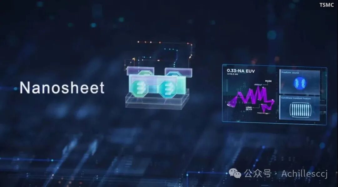 For decades, engineers have been carving atomic-scale machines on grains of sand. Chips are becoming smaller, faster, and more powerful, and we are on the verge of entering the Ångström era. However, there is an uncomfortable truth that no one wants to admit: this era is actually coming to an end. The semiconductor industry is hitting the hard limits of physics.。 Transistors are now only a few atoms wide, and they are becoming mechanically unstable. Heat is increasing exponentially. We are pinning our hopes on alternative materials, which are not advancing quickly enough. If we do not invent a new type of device and discover a real breakthrough, the computing revolution will come to a halt. Consequently, everything that relies on computing advancements will stagnate: technological progress, artificial intelligence, space technology, and even personal devices. All of this will hit a performance ceiling.
The Source of Future Semiconductor Technologies: IMEC in Belgium
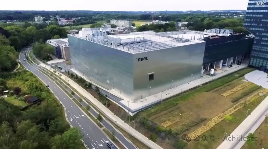 In this desperate moment, when the world’s largest tech companies like Apple, Google, NVIDIA, AMD, and even TSMC are at a loss, they turn to a place—a small lab in Belgium that hardly anyone has heard of. The future of computing is being invented here. If you trace any advanced chip, from AMD or NVIDIA to Apple chips, the source is not in Silicon Valley or Taiwan, but in a quiet town called Leuven in Belgium, home to IMEC.。 This is not a typical chip manufacturer. It is a research center dedicated to developing advanced technologies that chip manufacturers like TSMC, NVIDIA, Samsung, and Intel will use in 10 to 20 years. Here, seemingly impossible physical problems have already been turned into workable prototypes long before they appear in Apple or NVIDIA’s keynote speeches.
Modern Devices Run on FinFETs
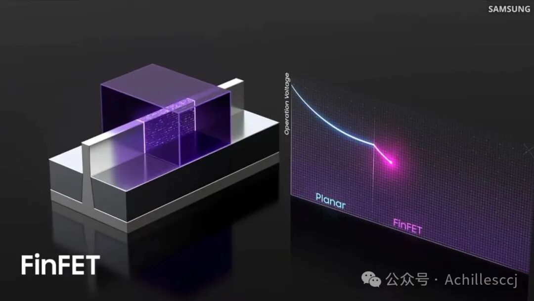 All modern devices operate on FinFETs (Fin Field-Effect Transistors). FinFET devices have supported a decade of technological advancements, from the first Apple chip to the GPUs powering the most advanced data centers on Earth. But its era is coming to an end. To continue shrinking transistors, the key structure within them—the fins—must become thinner and thinner, possibly only 6 nanometers wide and 60 nanometers high, and they tend to bend and break during manufacturing.。
IMEC’s Proposed GAA Structure is Entering Next-Generation GPUs and Smartphones
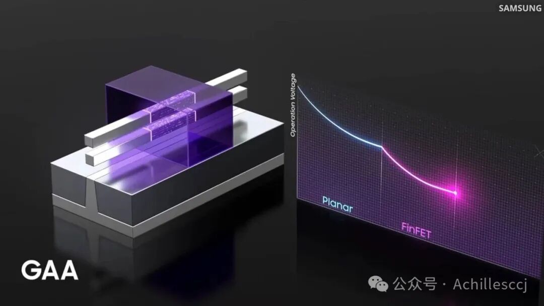 When challenges become too complex, expensive, and risky to solve alone, giants like Intel, Samsung, ASML, and TSMC collaborate with IMEC. They want to ensure that the billions of dollars they are about to invest are not going in the wrong direction.。 IMEC has explored every path they could think of, including new materials, new architectures, and new shapes. Most attempts have ended in failure. Ultimately, they arrived at a solution: instead of using tall fins, they stack thin sheets horizontally, supported from below to make them more stable. This is the Gate-All-Around (GAA) transistor. These devices are now entering next-generation GPUs and smartphones.
Next-Generation Transistor: CFET
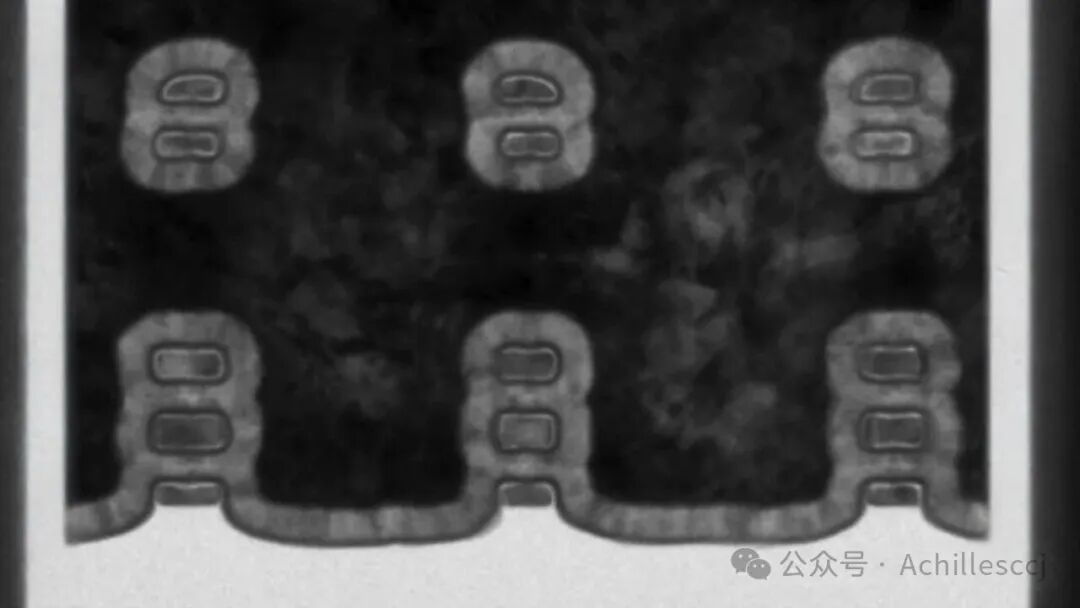 But this is not the end, because even with GAA transistors, space on chips remains tight, and IMEC has to look for new solutions again. IMEC proposed a bold idea: if we can no longer shrink transistors in the 2D plane, we must go up. By stacking one device vertically on top of another, the transistor density doubles instantly.。 For CFETs (Complementary Field-Effect Transistors), IMEC explored various methods of stacking transistors. Most failed, but one solution showed promise and became the path forward. For the first time in history, we are starting to build chips in 3D dimensions.
Scanning Electron Microscope (SEM): Seeing Structures at 10 Nanometers
One of the coolest machines at IMEC is the Scanning Electron Microscope (SEM). This is the only way to see the structure of transistors. You cannot actually “see” structures at 2 nanometers or even 10 nanometers. Our eyes only work when light reflects off an object. But for such small things, light waves are too large. The wavelength of light is several hundred nanometers wide. This is why ordinary optical microscopes are almost useless for viewing transistors. We need a scanning electron microscope.。 First, the wafer is placed in a chamber. Inside, a fine beam of electrons scans the surface of the chip. This allows us to magnify it hundreds of thousands of times. At first, what you see looks like simple lines. But when magnified 20,000 times, 50,000 times, or 150,000 times, patterns begin to emerge. The image shows the metal contacts leading to the device, which act like miniature highways for transmitting electrical signals into the transistor. When the electron beam hits the surface of the chip, it instantly heats up. If it stays on one point for even half a second, the electron beam will destroy the sample. There are only a few chances before it disappears.
Transmission Electron Microscope (TEM): Seeing the Internal Structure of Transistors
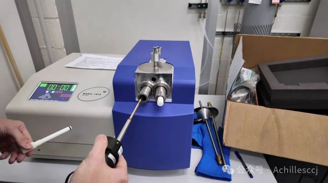 Even this super microscope has its limitations, as it can only magnify up to 10 nanometers. To observe nanosheet channels at the atomic level, another machine at IMEC is needed: the Transmission Electron Microscope (TEM). This machine can achieve magnifications of up to 50 million times. Just this machine took over a decade to build and cost hundreds of millions of dollars.。
Internal Structure of CFET
Before observing, the chip must be sliced and placed on a copper grid, then loaded into the microscope. The thickness of the slice cannot exceed 30 nanometers; if it is thicker, electrons cannot pass through. When magnified in the device, the structure of the CFET transistor can be seen.。 Now finally, we are going to magnify and observe the CFET transistor. The screen shows metals, contacts, and gates. The gray areas are silicon and silicon-germanium. Running through the image, like a fine line, is the nanosheet channel. This is the tiny path through which current flows when the transistor is turned on. The top is the P-type channel, and the bottom is the N-type channel.
Continuing to Magnify Reveals Individual Atoms
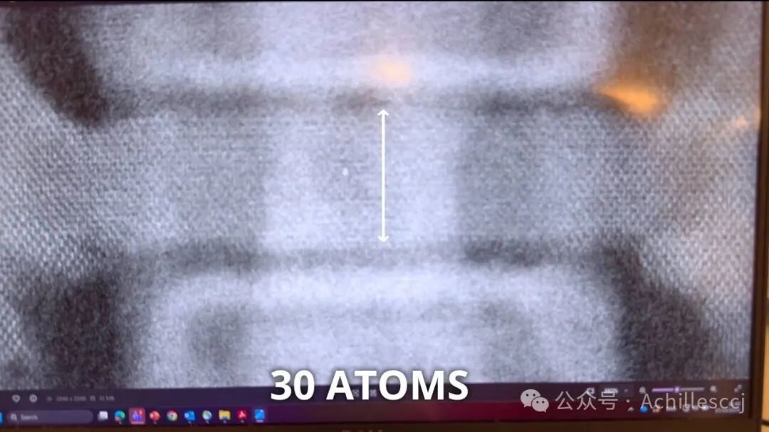 For the first time in history, two transistors are stacked vertically, encapsulating more power in a smaller space, ushering in a new era of computing.。 If we continue to magnify, we can see individual atoms in the channel. This channel is only about 30 atoms thick, which is the physical limit of reality.
Thousands of Steps in Chip Manufacturing Require Structural Inspection
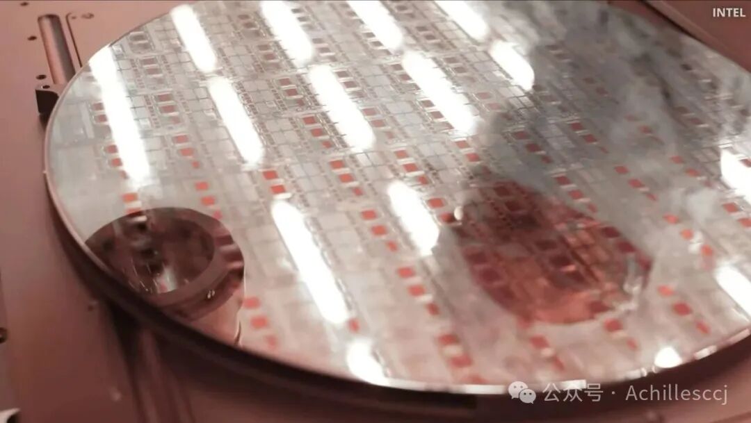 The process of observing devices using SEM and TEM involves firing electrons at the device, risking its destruction every second. These devices are not only expensive but also require extensive training. However, they are intuitively important for chip development. Modern chip manufacturing involves layer upon layer of constructing these tiny structures, comprising thousands of steps. At each stage, engineers need to check whether the structure is still perfect and whether any issues have arisen. If problems occur, they need to identify the cause and fix the process.。
Moore’s Law is a Law of Device Capability
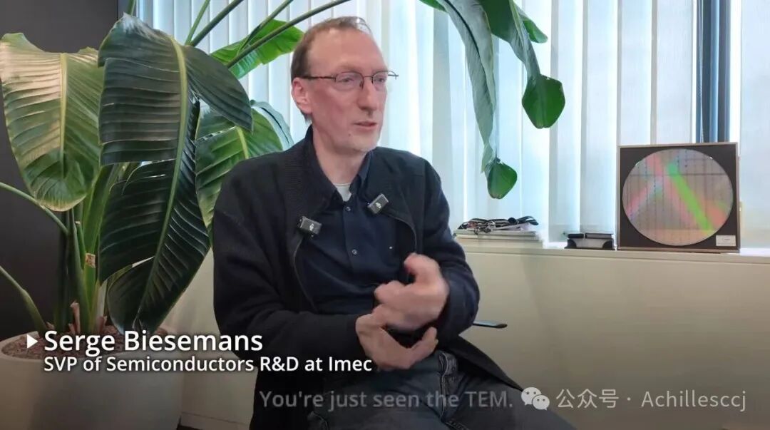 Most people think that new chip technologies appear out of thin air every few years, but the reality is quite different. In fact, it takes 18 to 20 years from the conception of a new transistor to its eventual entry into your phone. Designing transistors is one of the toughest engineering challenges on Earth. Serge Biesemans leads the invention of CFET technology at IMEC, and he is effectively leading the innovations that NVIDIA, TSMC, Intel, and Apple will rely on in the next decade. Just to achieve TEM images took them four years.。 He mentioned that the new CFET structure is not simply three times the aspect ratio of FinFETs; even if a perfect design is created, if the tools cannot physically manufacture it, that design will perish. Because in the semiconductor industry, new devices are not just a design challenge but also a tool challenge. In a sense, Moore’s Law is a law of device capability.
CFET Requires a New Set of Technologies
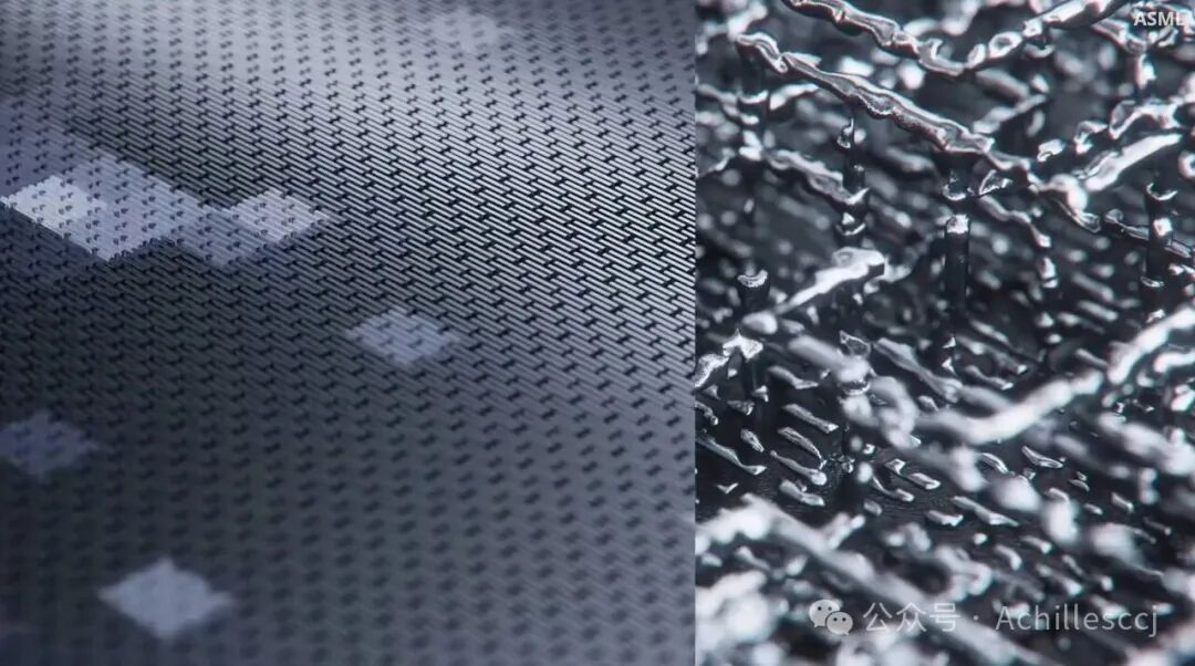 The invention of CFET demands higher tool requirements than ever before. To stack two transistors together, an entire generation of new tools is needed. You must be able to precisely etch and construct tall, narrow structures without letting them collapse; you must grow and remove materials layer by layer without damaging anything underneath; and you must be able to power from the back of the wafer.。
IMEC Works Closely with Tool Manufacturers
 These are things that have never been done before, requiring new etching and deposition systems, new epitaxy techniques, new back-powering processes, and most importantly, new tools capable of measuring those previously “invisible” details. This is why IMEC collaborates closely with tool manufacturers like ASML, key edge deposition and epitaxy (EPI) suppliers, and critical materials suppliers to develop the equipment and materials needed to turn these ideas into reality.。 These tools are not cheap. Just the unit price of EUV exceeds $250 million. Most other equipment ranges from $10 million to $50 million. And to run even a single experimental wafer production line requires about 200 such devices. Once the early versions of these tools are released, they do not go directly to TSMC or Intel; they first come to IMEC. Researchers will test them directly on silicon wafers.。
No Clear Roadmap After CFET
 To make CFET a reality, new tools, materials, and technologies must work in perfect synchronization. While the journey to make CFET mass-producible is ongoing, IMEC is already researching what comes after CFET. Because in the semiconductor industry, if you wait until the current technology runs out of steam to start, it will be too late.。 CFET has bought the semiconductor industry ten more years. But the future remains uncertain. For the first time in chip history, there is no clear roadmap after CFET. The only certainty is that CFET cannot reduce power consumption or heat generation sufficiently to meet future AI demands. We need more to break the physical laws that limit silicon itself.。
The Future May Involve Stacking More Layers
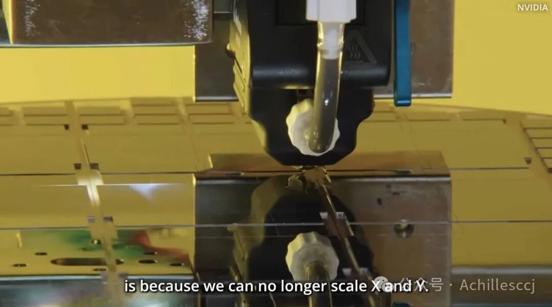 Regarding what comes after CFET, Serge Biesemans can only think of one thing: we start stacking more layers. There are no more ideas to easily expand in the X and Y axes; we must utilize the vertical dimension, and CFET is just the first generation of learning how to do that. If we master this in the mid-2030s of the next decade, Serge Biesemans believes it will open up space for mixed channels and mixed technologies.。
The History of Digital Computing
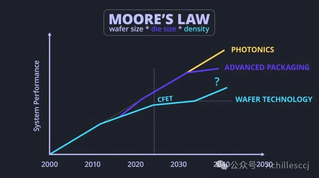 The initial progress in computing history came from shrinking transistors. Around 2020, the physics of making smaller transistors began to plateau: costs exploded, heat generation skyrocketed, and it became difficult to shrink sizes quickly. CFET will extend this line a bit further, possibly taking us to 2030, but it cannot restore exponential growth.。 Industries are forced to redefine Moore’s Law; if transistors cannot be improved, the entire system must be improved. Now, many companies no longer build a single massive chip but combine multiple smaller chips side by side or even vertically. The performance of chips comes not only from smaller transistors but also from how fast chiplets can communicate with each other. Currently, chiplets on a chip are only a few centimeters apart. At this distance, communication is like shouting across a football field. This wastes energy and slows everything down. A promising solution is to have these chiplets communicate using light instead of electricity, which is silicon photonics.
IMEC is Working to Improve the Efficiency of Silicon Photonics Technology
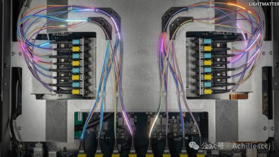 Currently, the power consumption of silicon photonics technology is still too high to be used everywhere, especially inside laptops and smartphones. Lasers generate significant heat, waste energy, and the entire system is extremely sensitive to temperature. Typically, heaters are needed to keep the light stable, which somewhat contradicts the energy-saving purpose.。 This is where IMEC comes in. They are not trying to prove that silicon photonics is feasible; they are working to make it efficient enough to be used everywhere. Currently, they are experimenting with various advanced optical materials, some of which are optically very interesting but incompatible with wafer fabrication.。
Committed to Stacking Entire Wafers Together
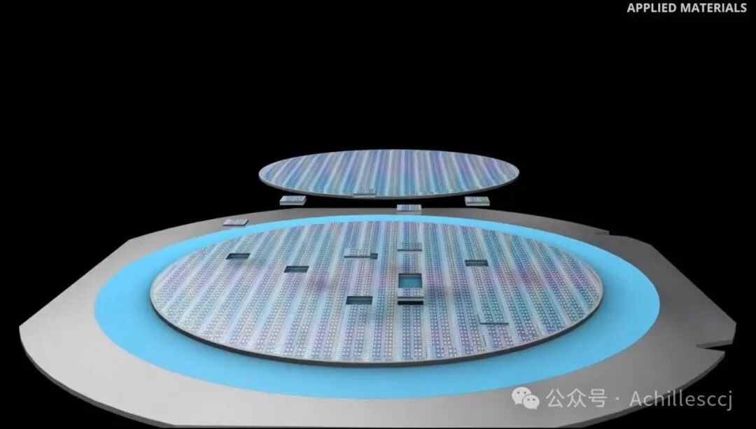 IMEC’s vision goes far beyond this. They are currently working on stacking entire wafers together. Imagine perfectly stacking two cities on top of each other, with every street aligned. If this can be achieved, most of the communication lines between chips can be eliminated. This means lower power consumption, higher speeds, and most importantly, the ability to stack different types of chips and materials, not just silicon. Chips will no longer be flat but will resemble a 3D computing cube.。
IMEC’s Multiple Teams are Racing in Parallel
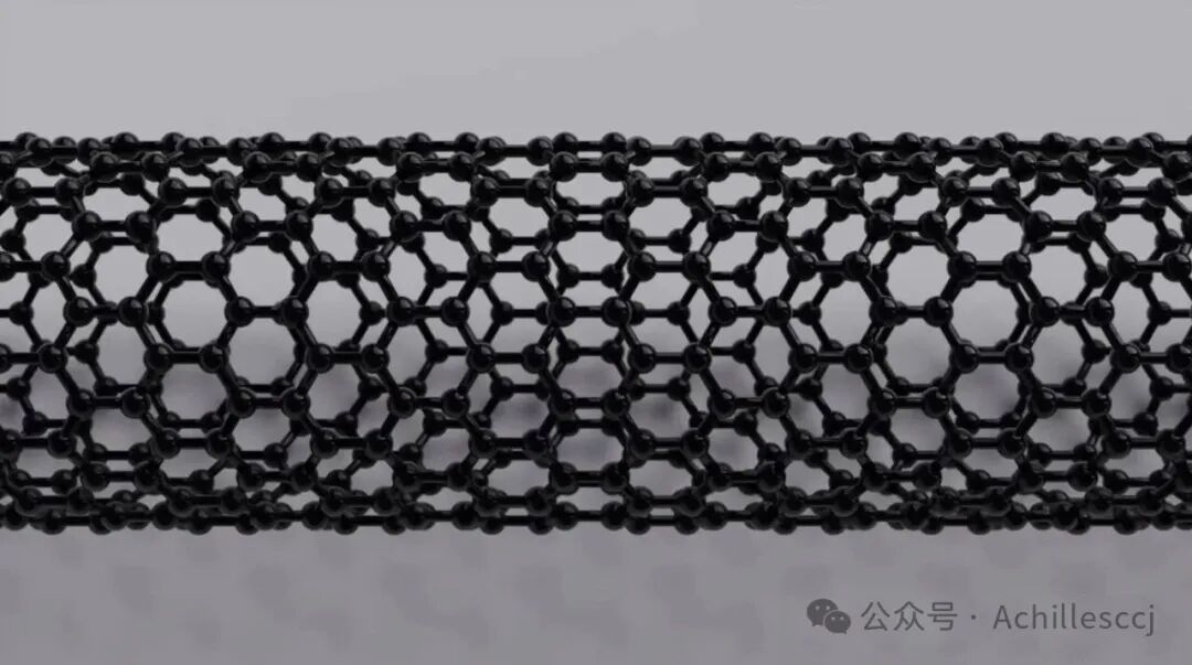 IMEC is not betting on just one future. Currently, they have multiple teams racing in parallel, each exploring a completely different path to discover what might come after silicon; no one knows which path will succeed. They are currently testing ternary logic, reversible logic, spintronics, and low-temperature CMOS. Ultimately, we may need a completely new device that follows different physical laws than those followed by silicon.。 They are also experimenting with germanium, graphene, 2D materials like transition metal dichalcogenides, and even carbon nanotubes, which are only a few atoms thick. They are trying to transform these tiny lab samples into technologies that can be produced on a large scale.。 What makes IMEC unique is not just its engineers, tools, and partners, but also its neutrality. IMEC is non-profit and does not compete with anyone. It is not just a laboratory but a global hub for the next generation of chips. The future is not predetermined. IMEC, along with its partners, is racing against time, energy, and the limits of physics itself.