In the electronics industry, printed circuit boards (PCBs) play a crucial role, and the outer layer processing of PCBs is a key factor that determines their performance and quality. It not only relates to the functionality of the circuit board but also directly affects the reliability and durability of the product. This article will detail the process of PCB outer layer processing, the materials required, key control points, and the main defects that may occur.
1. Process
-
Pre-treatment
-
The purpose is to remove oxides, oils, and other impurities from the copper surface to ensure good adhesion in subsequent processes. Chemical cleaning or mechanical brushing is typically used.
-
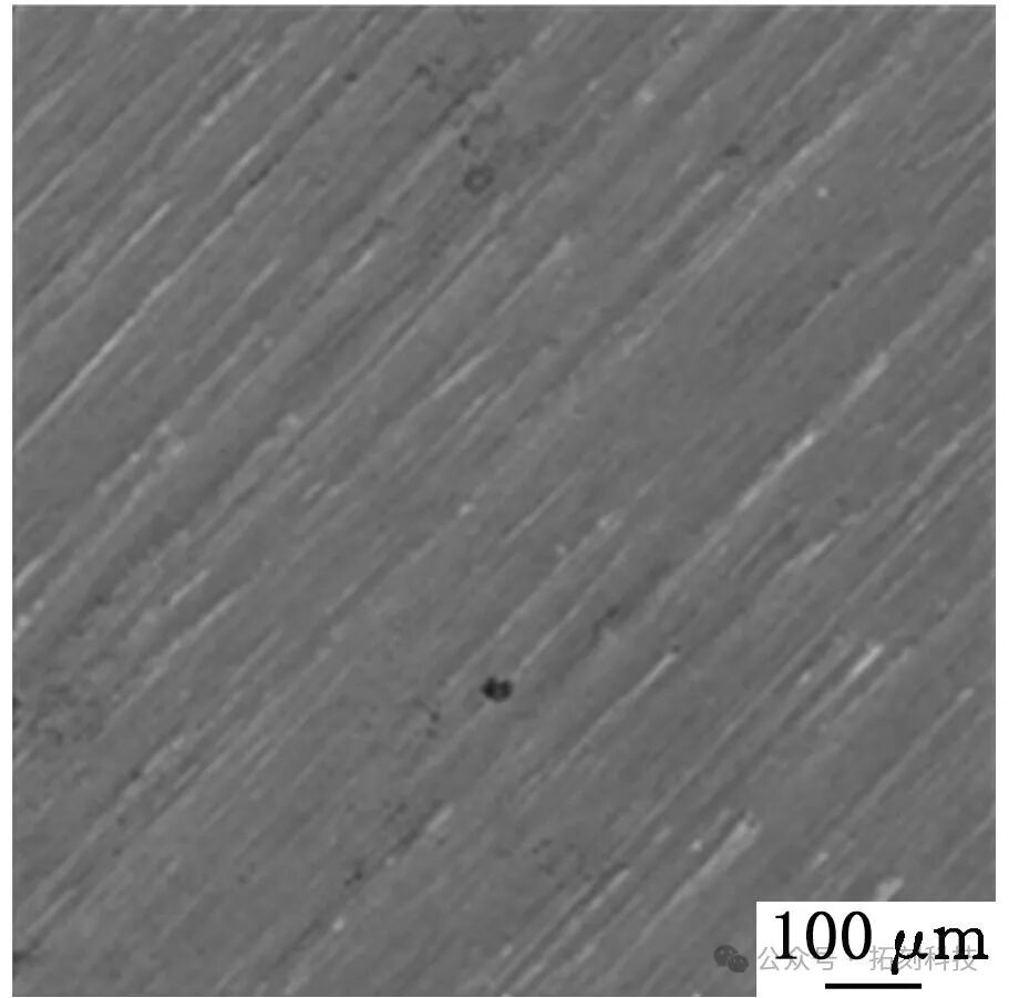
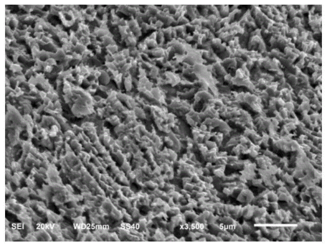
Currently, all manufacturers have adopted a method of first mechanical brushing (the non-woven brush wheel mentioned in the previous article) followed by chemical micro-etching (medium or coarse etching), which ensures a clean copper surface while avoiding small brush marks that could affect yield.
-
During this process, it is essential to strictly control the concentration, temperature, and treatment time of the cleaning solution to avoid over-cleaning or incomplete cleaning.
-
The left image below is an electron microscope photo of mechanical brushing, and the right image shows the copper surface after coarse etching.
Film Lamination
-
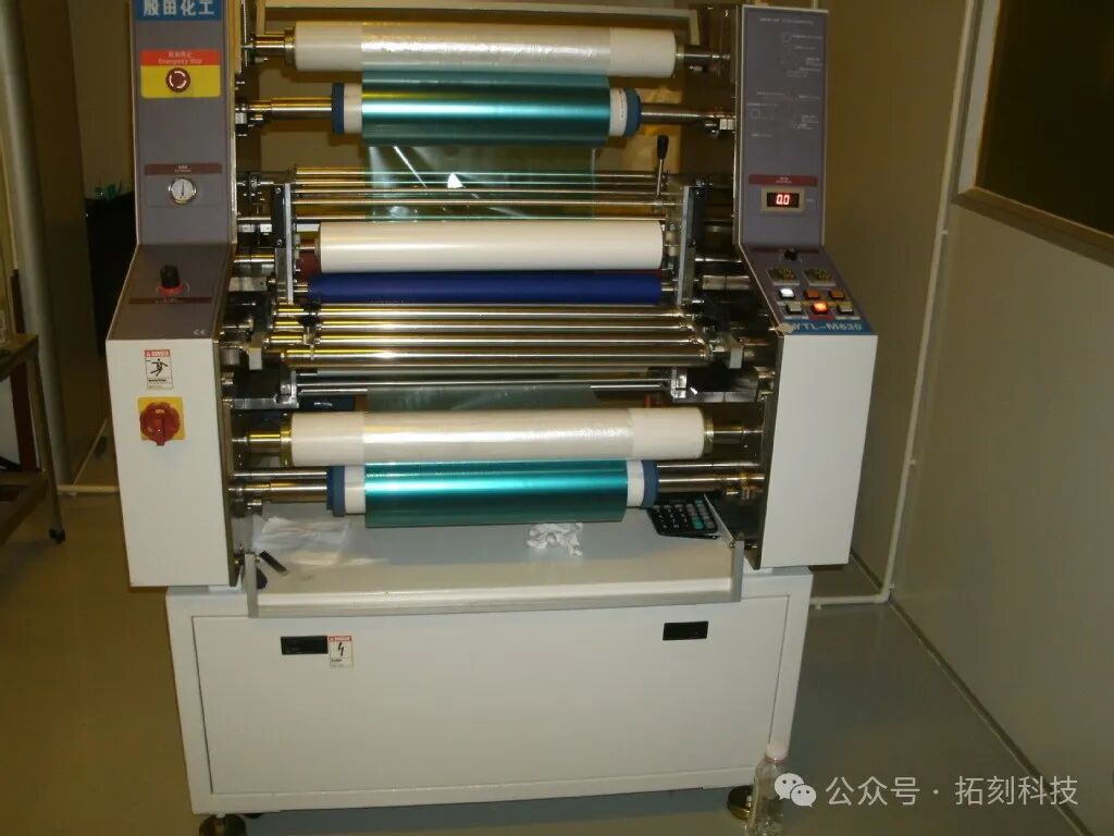
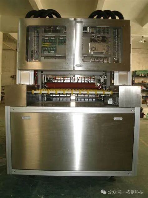
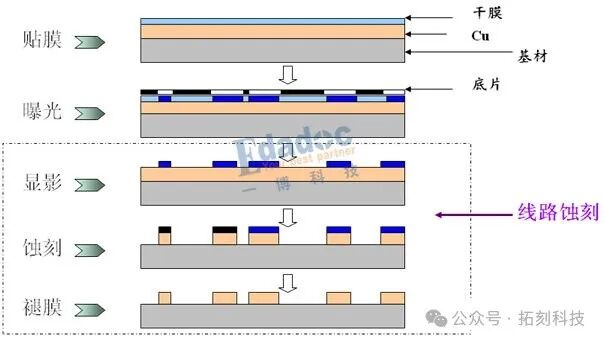
Dry film (a type of photosensitive material) is uniformly pressed onto the surface of the PCB. The choice of dry film should be based on the design requirements and process characteristics of the PCB, ensuring it has good resolution, adhesion, and corrosion resistance. In simple terms, it should be selected based on line width, spacing, and PTH hole size.
-
The pressure, temperature, and speed of the lamination are critical parameters that need to be precisely controlled to ensure a tight bond between the dry film and the copper surface.
Exposure
-
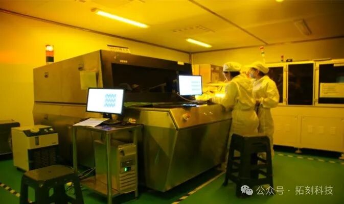
Choose an appropriate exposure machine based on the selected dry film, for example, LDI-specific dry film must use LDI machines, while ordinary dry film can use CCD exposure machines.
-
If using LDI or DI exposure, no film is needed. However, if using a traditional CCD exposure machine, film or glass plates are still required. The pre-designed circuit pattern is projected onto the PCB with the dry film, causing a chemical reaction in the dry film.
-
-
Exposure energy, time, and alignment are critical factors affecting exposure quality. Insufficient exposure can lead to unclear patterns, while excessive exposure can cause over-hardening of the dry film, affecting subsequent development and etching.
-
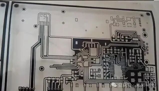
Here we are discussing the Panel Plating process, so the exposure pattern will differ from Pattern Plating. Below is the Panel Plating outer layer film, where you can see that the lines are blank, and after exposure, the dry film protects the copper surface from etching.
Development
-
Use a developer solution to remove the unexposed dry film, revealing the copper surface that needs to be etched. The concentration, temperature, and development time of the developer solution must be strictly controlled to ensure the accuracy and integrity of the pattern.
-
After development, the PCB needs to be inspected to promptly identify and address any development issues.
Etching
-
Place the developed PCB into an acidic etching solution to etch away the copper not protected by the dry film, forming the circuit pattern. The composition, temperature, and etching speed of the etching solution are critical parameters that need to be adjusted based on different PCB designs and materials.
-
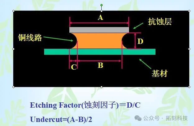
During the etching process, closely monitor the etching effect to prevent over-etching or under-etching. In addition to checking for unetched areas between lines, a very important indicator is the etching factor.
Stripping
-
After etching, use a stripping solution to remove the dry film, revealing the final circuit pattern. The choice and use of the stripping solution must be careful to avoid damaging the PCB.
Post-treatment
-
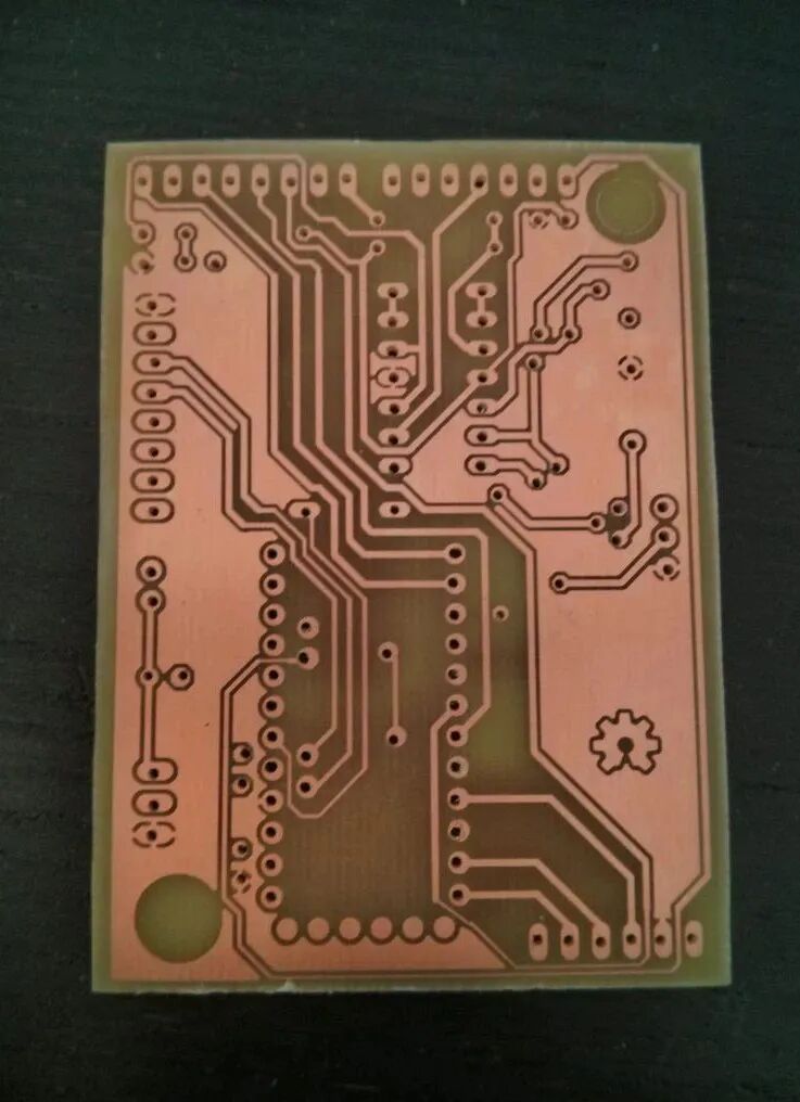
This includes cleaning, drying, and anti-oxidation treatments to ensure the appearance and performance of the PCB. During post-treatment, it is essential to strictly control the composition and temperature of the cleaning solution, as well as the time and temperature of drying. The final product looks like this.
2. Materials
-
Dry Film
-
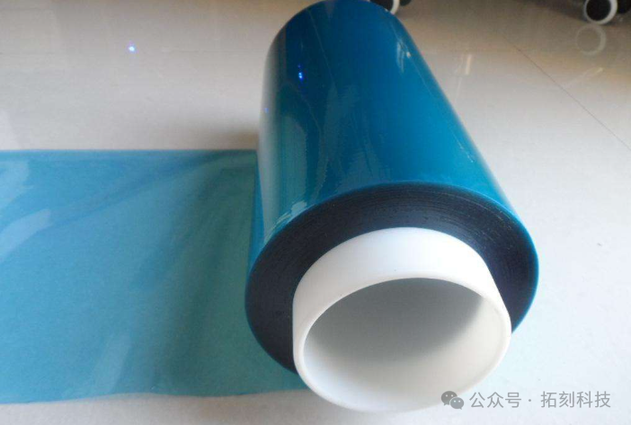
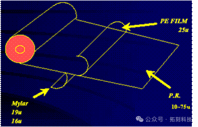
Dry film is a key material in the PCB outer layer process, consisting of a polyester film, photosensitive layer, and protective film. The performance of the photosensitive layer directly affects the quality and precision of the PCB pattern.
-
When selecting dry film, factors such as resolution, adhesion, corrosion resistance, and temperature resistance must be considered. The dry film is rolled and has strict storage and usage conditions; it consists of three layers, and during automatic film application, the machine automatically tears the PE film while pressing the dry film onto the board. After exposure and before development, the mylar must be removed (most factories still use manual mylar removal, which is a significant source of quality issues).
Exposure Machine
-
The exposure machine is used to expose the circuit pattern onto the dry film. Different types of exposure machines have different characteristics and applications, such as parallel light exposure machines and scattered light exposure machines.
-
The light intensity, uniformity, and alignment of the exposure machine are critical parameters for exposure quality.
Etching Solution
-
The composition and performance of the etching solution determine the speed and effect of etching. Common etching solutions include ferric chloride etching solution and acidic copper chloride etching solution.
-
The concentration, temperature, and pH of the etching solution need to be adjusted based on the PCB’s materials and design requirements.
3. Key Control Points
-
Environmental Control
-
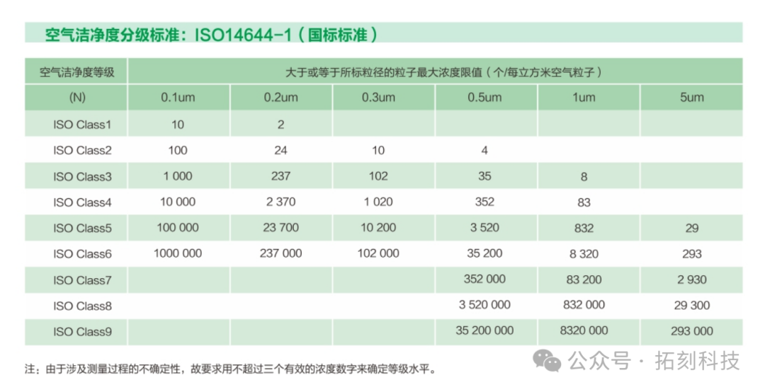
The outer layer processing of PCBs requires a high standard of environmental control, maintaining a clean, temperature-controlled, and humidity-controlled production environment. Dust and humidity in the air can affect the adhesion of the dry film and the quality of exposure.
-
The production workshop should use an air purification system, strictly control temperature and humidity, and regularly clean and maintain the environment.
-
Therefore, the general requirement for the outer layer cleanroom is at least a class 10,000 (ISO 7) standard.
Equipment Maintenance
-
The outer layer process involves many pieces of equipment, such as exposure machines, etching machines, and lamination machines. The performance and stability of these devices directly affect the quality of the PCB.
-
Regular maintenance and servicing of the equipment are necessary, checking all parameters to ensure they are normal, and timely replacement of worn parts to ensure good operation.
-
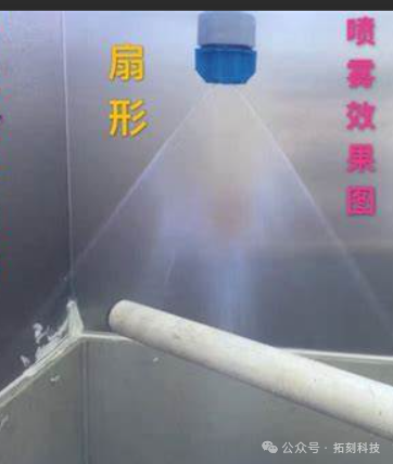
Key equipment includes the lamination machine for debris, internal dirt in the exposure machine, and nozzle blockage in the etching machine.
Process Parameter Control
-
Strictly control all process parameters in the outer layer processing, such as cleaning solution concentration, lamination pressure, exposure energy, and etching speed. Even minor changes in process parameters can lead to fluctuations in PCB quality.
-
Establish a comprehensive monitoring system for process parameters, regularly testing and adjusting them to ensure stability and consistency in the process.
Quality Inspection
-
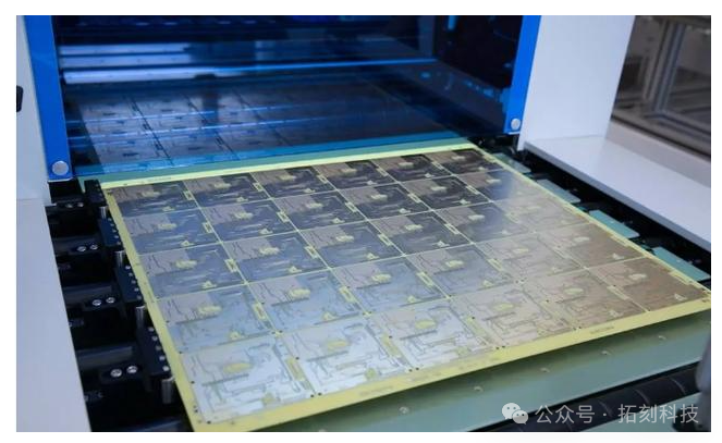
Mainly through AOI for inspecting the etched circuit.
4. Major Defects
-
Poor Exposure
-
Manifested as unclear patterns, overexposure or underexposure, and alignment deviations. Causes may include improper exposure machine parameter settings, quality issues with the photomask, and unstable dry film quality.
-
Solutions include adjusting exposure machine parameters, replacing the photomask, and selecting higher quality dry film.
Poor Etching
-
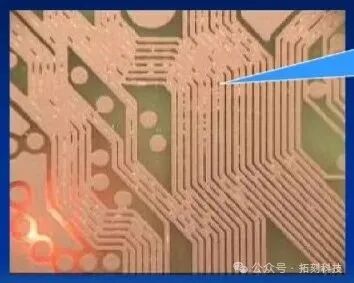
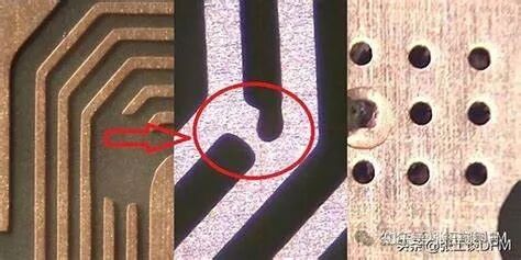
Main issues include over-etching, under-etching, and side etching. Causes may include inappropriate etching solution parameters, excessive or insufficient etching time, and equipment malfunctions.
-
Adjusting etching solution parameters, controlling etching time, and repairing etching equipment can improve etching quality.
Poor Adhesion of Dry Film
-
Insufficient adhesion between the dry film and copper surface can easily lead to pattern detachment. Causes may include inadequate pre-treatment, improper lamination parameters, and dry film quality issues.
-
Improving pre-treatment, optimizing lamination parameters, and replacing dry film can enhance adhesion.
Poor Appearance
-
Such as scratches, stains, and oxidation. These may be caused by improper operations during production, unclean environments, and inadequate post-treatment.
-
Standardizing operational procedures, maintaining a clean production environment, and enhancing post-treatment can reduce the occurrence of appearance defects.
In summary, the PCB outer layer process is a complex and critical step that requires strict control over processes, materials, key control points, and defects to ensure that the quality and performance of PCBs meet the demands of the electronics industry.