In recent years, due to the demand and growth of Bluetooth devices, Wireless Local Area Network (WLAN) devices, and mobile phones, practitioners have increasingly focused on RF circuit design techniques. From the past to the present, RF circuit board design has been as difficult for engineers to master as electromagnetic interference (EMI) issues, even a nightmare. To achieve successful design at once, careful planning and attention to detail are essential.
RF circuit board design is often described as a “black art” due to the many uncertainties in theory. However, this is an overly general view; there are indeed many rules that can be followed in RF circuit board design. Nevertheless, in practical design, the truly useful techniques come into play when these rules cannot be implemented due to various constraints. Key RF design topics include: impedance and impedance matching, insulating layer materials and stacked boards, wavelength and harmonics… This article will focus on various issues related to RF circuit board partition design.
Types of Microvias
Different types of circuits on a circuit board must be separated, yet they need to connect in the best way without causing electromagnetic interference, which requires the use of microvias. Microvias typically have a diameter of 0.05mm to 0.20mm, which are generally categorized into three types: blind vias (blind via), buried vias (bury via), and through vias (through via). Blind vias are located on the top and bottom surfaces of the printed circuit board and have a certain depth, used for connecting surface lines with inner layer lines below, and the depth of the hole usually does not exceed a certain ratio (hole diameter). Buried vias refer to connection holes located within the inner layers of the printed circuit board and do not extend to the surface of the board. The aforementioned two types of holes are located in the inner layers of the board and are completed using through-hole forming processes before lamination, and during the via formation process, several inner layers may overlap. The third type, through vias, passes through the entire circuit board and can be used for internal interconnections or as adhesive positioning holes for components.
Using Partition Techniques
When designing RF circuit boards, high-power RF amplifiers (HPA) and low-noise amplifiers (LNA) should be isolated from each other as much as possible. Simply put, this means keeping high-power RF transmitting circuits away from low-power RF receiving circuits. If there is plenty of space on the PCB board, this can be easily achieved. However, when there are many components, the space on the PCB becomes limited, making this difficult to achieve. They can be placed on opposite sides of the PCB or allowed to operate alternately rather than simultaneously. High-power circuits may also include RF buffers (buffer) and voltage-controlled oscillators (VCO).
Design partitioning can be divided into physical partitioning (physical partitioning) and electrical partitioning (Electrical partitioning). Physical partitioning mainly involves component layout, orientation, and shielding issues; electrical partitioning can further be divided into power distribution, RF routing, sensitive circuits and signals, grounding, etc.
Physical Partitioning
Component layout is key to achieving excellent RF design. The most effective technique is to first fix the components located on the RF path and adjust their orientation to minimize the length of the RF path. Furthermore, keep RF inputs away from RF outputs and as far away as possible from high-power and low-power circuits.
The most effective board stack method is to arrange the main ground on the second layer beneath the surface layer, and keep the RF lines on the surface layer as much as possible. Minimizing the size of vias on the RF path not only reduces path inductance but also minimizes virtual solder points on the main ground and reduces the opportunity for RF energy to leak into other areas of the stacked board.
In physical space, linear circuits like multi-stage amplifiers are usually sufficient to isolate multiple RF zones from each other, but duplexers, mixers, and intermediate frequency amplifiers always have multiple RF/IF signals interfering with each other, so care must be taken to minimize this impact. RF and IF routing should cross as much as possible and be separated by a ground area between them. Correct RF paths are crucial for the performance of the entire PCB board, which is why component layout often takes up most of the time in mobile phone PCB design.
On mobile phone PCB boards, low-noise amplifier circuits can often be placed on one side of the PCB, while high-power amplifiers are placed on the other side, ultimately connecting them to one end of the RF antenna and the other end of the baseband processor via a duplexer on the same side. This requires some skill to ensure that RF energy does not transfer from one side of the board to the other via vias, a common technique is to use blind vias on both sides. The adverse impact of vias can be minimized by arranging blind vias in areas on both sides of the PCB that are not affected by RF interference.
Metal Shielding
Sometimes, it is not feasible to maintain sufficient separation between multiple circuit blocks; in such cases, it is necessary to consider using metal shielding to confine RF energy within RF areas. However, metal shielding also has side effects, such as high manufacturing and assembly costs.
Irregularly shaped metal shields are difficult to guarantee high precision during manufacturing, while rectangular or square metal shields can impose some restrictions on component layout; metal shields are not conducive to component replacement and fault relocation; since metal shields must be soldered to the grounding surface and must maintain a proper distance from components, they occupy valuable PCB board space.
It is crucial to ensure the integrity of the metal shield, so digital signal lines entering the metal shield should run as much as possible on the inner layers, and it is best to set the next layer of the signal routing layer as a grounding layer. RF signal lines can be routed out from small notches at the bottom of the metal shield and grounding notches, but the areas around the notches should be surrounded by a large grounding area, and grounding on different signal layers can be connected together through multiple vias.
Despite the above drawbacks, metal shielding remains very effective and is often the only solution for isolating critical circuits.
Power Decoupling Circuit
Additionally, a proper and effective chip power decoupling (decouple) circuit is also very important. Many RF chips integrated with linear lines are very sensitive to power noise, usually requiring each chip to use up to four capacitors and an isolation inductor to filter out all power noise. (Figure 1)
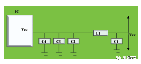
The minimum capacitance value usually depends on the resonant frequency of the capacitor itself and the lead inductance, C4 is chosen based on this. C3 and C2 values are relatively larger due to their own lead inductance, resulting in a poorer RF decoupling effect, but they are more suitable for filtering lower frequency noise signals. RF decoupling is accomplished by the inductor L1, which prevents RF signals from coupling into the chip from the power line. Since all routing can act as a potential antenna that can receive and transmit RF signals, isolating RF signals from critical lines and components is essential.
The physical location of these decoupling components is also critical. The layout principle for these important components is: C4 should be as close as possible to the IC pins and grounded, C3 must be closest to C4, C2 must be closest to C3, and the connection route between IC pins and C4 should be as short as possible. The grounding ends of these components (especially C4) should typically connect to the first grounding layer beneath the board surface and the chip’s grounding pin. The vias connecting the components to the grounding layer should be as close as possible to the component pads on the PCB board, and it is best to use blind vias punched on the pads to minimize lead inductance. Inductance L1 should be close to C1.
An integrated circuit or amplifier often has an open collector (open collector) output, thus requiring a pullup inductor (pullup inductor) to provide a high impedance RF load and a low impedance DC power supply. The same principle applies to decoupling the power end of this inductor. Some chips require multiple power supplies to operate, so two to three sets of capacitors and inductors may be needed to decouple them separately. If there is insufficient space around the chip, the decoupling effect may be poor.
It is especially important to note that: inductors should rarely be placed parallel to each other, as this will form an air-core transformer and induce interference signals, so the distance between them should be at least equal to one of their heights, or arranged at right angles to minimize mutual inductance.
Electrical Partitioning
The principles of electrical partitioning are essentially the same as those of physical partitioning but also include some other factors. Certain parts of modern mobile phones operate at different working voltages and are controlled by software to extend battery life. This means that mobile phones need to run multiple power supplies, which creates more isolation issues. Power is usually introduced via connectors (connector) and immediately undergoes decoupling to filter out any noise from outside the circuit board, then passes through a set of switches or regulators before power distribution.
In mobile phones, most circuits have relatively small DC currents, so routing width is usually not an issue. However, a separate wide current line must be designed for the power supply of high-power amplifiers to minimize voltage drop (voltage drop) during transmission. To avoid excessive current loss, multiple vias should be used to transfer current from one layer to another. Additionally, if sufficient decoupling cannot be achieved at the power pin of the high-power amplifier, high-power noise will radiate across the entire circuit board, causing various problems. The grounding of high-power amplifiers is quite important and often requires a metal shield to be designed for it.
RF Outputs Must Be Far from RF Inputs
In most cases, it is essential to ensure RF outputs are far from RF inputs. This principle also applies to amplifiers, buffers, and filters. In the worst-case scenario, if the outputs of amplifiers and buffers feed back to their inputs with appropriate phase and amplitude, they may produce self-oscillation. They may become unstable and add noise and intermodulation products (intermodulation products) to the RF signal.
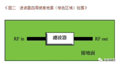
If the RF signal line loops back from the input of the filter to its output, this can severely damage the filter’s bandpass characteristics. To achieve good isolation between inputs and outputs, there must first be a large grounding area surrounding the filter, and secondly, the area beneath the filter must also be a grounding area, which must be connected to the main grounding surrounding the filter. It is also a good practice to keep the signal lines passing through the filter as far away from the filter pins as possible. Furthermore, careful attention must be paid to grounding throughout the entire circuit board; otherwise, an unwanted coupling channel may be inadvertently introduced. (Figure 2) illustrates this grounding approach in detail.
In some cases, single-ended (single-ended) or balanced RF signal lines (balanced RF traces) can be chosen, and the principles regarding crosstalk (crosstalk) and EMC/EMI also apply here. Balanced RF signal lines, if routed correctly, can reduce noise and crosstalk, but they typically have higher impedance. Moreover, to obtain a matched impedance signal source, routing, and load, a reasonable line width must be maintained, which can be challenging during actual routing.
Buffer
Buffers can be used to enhance isolation as they can split the same signal into two parts and drive different circuits. In particular, local oscillators may require buffers to drive multiple mixers. When mixers reach common mode isolation at RF frequencies, they will not function properly. Buffers can effectively isolate impedance variations at different frequencies, preventing interference between circuits.
Buffers are very helpful in design; they can be placed directly behind the circuits that need to be driven, resulting in very short high-power output lines. Since the input signal level of buffers is relatively low, they are less likely to interfere with other circuits on the board.
Voltage-Controlled Oscillator
A voltage-controlled oscillator (VCO) converts varying voltage into varying frequency, a feature used for high-speed channel switching. However, it also converts minute noise on the control voltage into small frequency variations, adding noise to the RF signal. In summary, once the RF output signal has been processed by the VCO, there is no way to eliminate the noise from it. The difficulty lies in the expected frequency bandwidth range of the VCO control line, which can range from DC to 2MHz, and it is nearly impossible to remove such a wide band of noise using filters; furthermore, the VCO control line is usually part of a feedback loop controlling frequency, which can introduce noise in many places, so it must be handled very carefully.
Resonant Circuit
The resonant circuit (tank circuit) is used in transmitters and receivers, and it relates to the VCO, but it also has its own characteristics. Simply put, a resonant circuit is made up of a series of diodes with inductance and capacitance connected in series, which helps set the operating frequency of the VCO and modulate voice or data onto the RF carrier.
All VCO design principles also apply to resonant circuits. Since resonant circuits contain a considerable number of components, occupy a large area, and typically operate at a high RF frequency, they are often very sensitive to noise. Signals are usually arranged on adjacent pins of the chip, but these signal pins need to work with larger inductances and capacitances, which requires placing these inductors and capacitors as close as possible to the signal pins and connecting them back to a control loop that is very sensitive to noise while avoiding noise interference. Achieving this is not easy.
Automatic Gain Control Amplifier
Automatic gain control (AGC) amplifiers are also a common source of problems, as both transmit and receive circuits will have AGC amplifiers. AGC amplifiers can effectively filter out noise, but because mobile phones can handle rapid changes in transmit and receive signal strength, the AGC circuit requires a relatively large bandwidth, making AGC amplifiers prone to introducing noise.
Designing AGC circuits must adhere to analog circuit design principles, namely using short input pins and short feedback paths, both of which must be kept away from RF, IF, or high-speed digital signal lines. Similarly, good grounding is essential, and the chip’s power supply must be well decoupled. If a long routing line must be designed at the input or output end, it is best to implement it at the output end, as the output end’s impedance is usually much lower than that of the input end, making it less likely to introduce noise. Generally, the higher the signal level, the easier it is to introduce noise into other circuits.
Grounding
It is crucial to ensure that the grounding beneath the RF routing layers is solid, and all components must be securely connected to the main ground and isolated from other routing that may introduce noise. Additionally, it is important to ensure that the power supply of the VCO is adequately decoupled, as the RF output of the VCO is often at a relatively high level, making it easy for VCO output signals to interfere with other circuits; hence, special attention must be given to the VCO. In fact, the VCO is often placed at the end of the RF area and may require a metal shield.
In all PCB designs, keeping digital circuits as far away from analog circuits as possible is a major principle, which also applies to RF PCB design. Common analog grounding and grounding used for shielding and separating signal lines are usually equally important. Similarly, RF lines should be kept away from analog lines and some critical digital signals; all RF routing, pads, and components should ideally be surrounded by grounding copper foil and connected to the main ground as much as possible. Microvias (microvia) constructed boards are useful during the RF routing development phase, as they allow for the use of many vias without incurring any costs; otherwise, drilling holes in regular PCB boards will increase development costs, which is not economical for mass production.
Placing a solid grounding area directly beneath the first layer provides the best isolation. Dividing the grounding area into several sections to isolate analog, digital, and RF lines does not work well, as there will always be some high-speed signal lines crossing these separated grounding areas, which is not a good design.
There are many issues related to signals and control lines that require special attention, but they are beyond the scope of this article.
Conclusion
Whether RF PCB design is a “black art” or not, adhering to some basic RF design rules and referencing excellent design examples will help complete RF design work. Successful RF design requires careful attention to every step and detail throughout the design process, meaning thorough and careful planning must be done at the start of the design phase, along with comprehensive and continuous evaluation of the progress of each design step. Such meticulous design skills are often lacking in the culture of most electronic companies in the country.
Note: This document is compiled from online sources for learning and sharing purposes. If there are any infringements, please contact us for deletion.