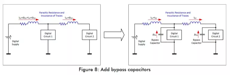
Digital circuits often require non-continuous current, which can cause surge currents in some high-speed devices.
If the power routing is long, the surge current can lead to high-frequency noise, which can then couple into other signals. In high-speed circuits, parasitic inductance, parasitic resistance, and parasitic capacitance are inevitable, so this high-frequency noise will eventually couple into other circuits.
Furthermore, the presence of parasitic inductance can reduce the maximum surge current that the routing can handle, leading to some voltage drop, which may disable the circuit.
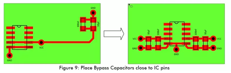
Therefore, it is particularly important to add bypass capacitors in front of digital devices. The larger the capacitance, the more limited its energy transmission is by the transmission rate, so it is generally combined with a large capacitor and a small capacitor to meet the requirements across the full frequency range.
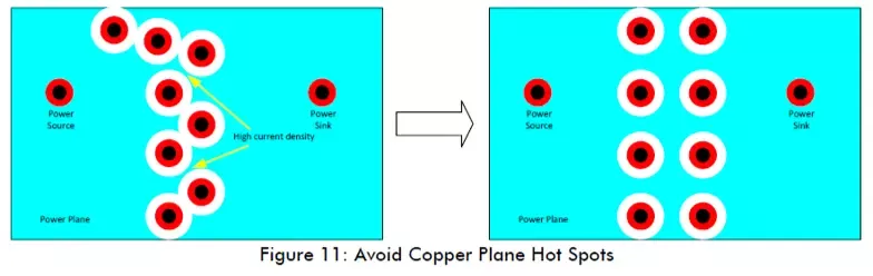
Avoiding Hotspots: Signal vias can create voids on the power and ground layers.
Improper placement of vias can significantly increase the current density in certain areas of the power or ground plane. These areas with increased current density are referred to as hotspots.
Thus, when setting vias, we must strive to avoid this situation to prevent the plane from being severed, which could ultimately lead to EMC issues.
Typically, the best way to avoid hotspots is to place vias in a mesh pattern, which ensures uniform current density, prevents isolation of the plane, and keeps the return path short, thus avoiding EMC problems.
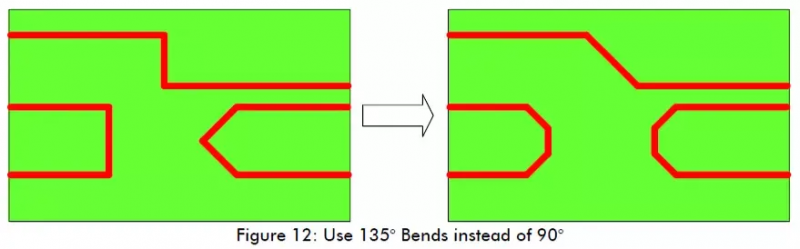
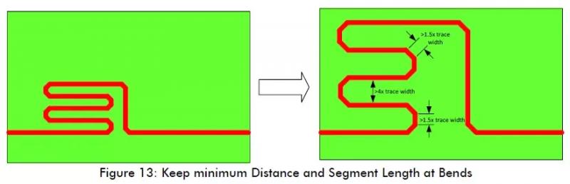
When routing high-speed signal lines, the signal lines should avoid bending as much as possible. If bending is unavoidable, it should not be sharp or at right angles; instead, it should use obtuse angles.
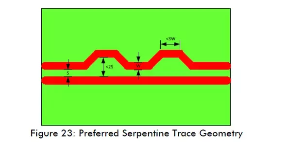
When routing high-speed signal lines, we often use serpentine routing to achieve equal length; this serpentine routing is also a form of bending.
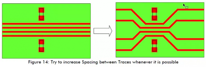
The line width, spacing, and bending methods should be chosen reasonably, and the spacing should meet the 4W/1.5W rule.
If high-speed signal lines are too close together, it is easy to produce crosstalk.
Sometimes, due to layout, board frame size, etc., the distance between high-speed signal lines exceeds our minimum required distance, in which case we can only try to increase the distance between high-speed signal lines at their bottleneck. If space permits, we should try to increase the distance between the two high-speed signal lines.
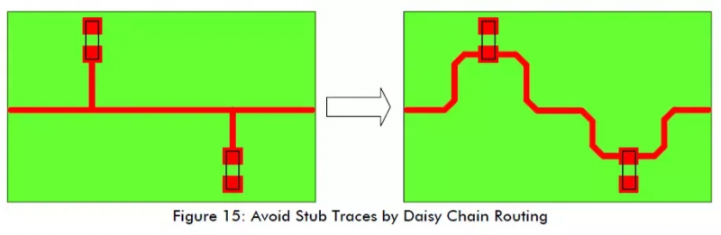
Long stub lines act like antennas, and if not handled properly, can cause serious EMC issues. Stub lines can also cause reflections, reducing signal integrity.
When adding pull-up or pull-down resistors on high-speed signal lines, stub lines are most easily generated, and generally, the way to handle stub lines is to use daisy chaining.
According to experience, if the length of the stub line is greater than 1/10 of the wavelength, it can be treated as an antenna, which then becomes a problem.
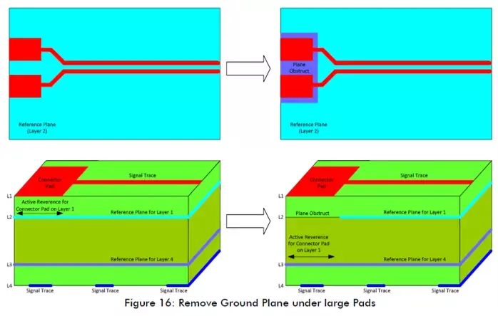
The impedance of a routing line generally depends on its width and the distance between the routing line and the reference plane. The wider the routing line, the smaller the impedance. This principle also applies to the pads of some interface terminals and devices.
When a pad of an interface terminal connects to a high-speed signal line, if the pad is particularly large while the high-speed signal line is particularly narrow, the large pad will have low impedance, whereas the narrow routing line will inevitably have high impedance; in this case, impedance discontinuity will occur, leading to signal reflections.
To solve this problem, a ground copper plane is usually placed under the large pad of the interface terminal or device, while placing the reference plane of the pad on another layer to increase the impedance, ensuring continuity of impedance.
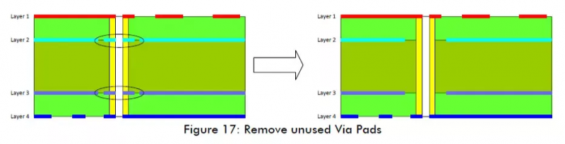
Vias are another source that can cause impedance discontinuity. To minimize this effect, unnecessary copper planes connected to the inner layer and vias should be removed. Such operations can actually be eliminated during design using CAD tools or by coordinating with PCB manufacturers to remove unnecessary copper planes, ensuring impedance continuity.
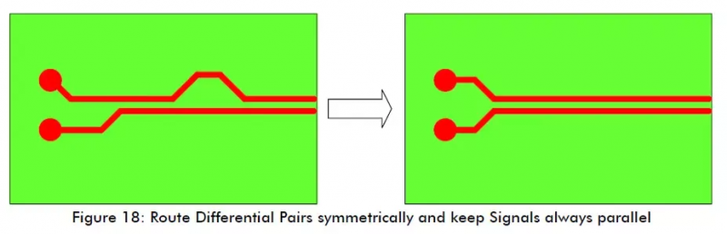
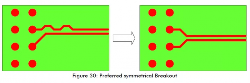
For high-speed differential signal lines, we must ensure equal width and equal spacing to achieve specific differential impedance values. Therefore, when routing differential signal lines, symmetry should be maintained as much as possible.
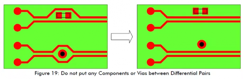
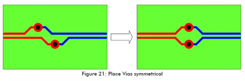
In the differential pair, avoid placing vias or components. If vias or components are placed in the differential pair, it can cause EMC issues and also lead to impedance discontinuity.
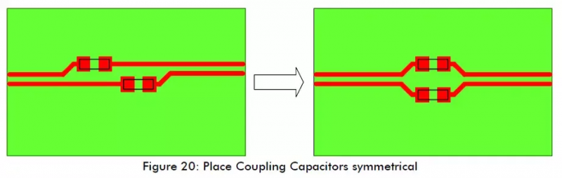
Sometimes, high-speed differential signal lines need to be connected with coupling capacitors. These coupling capacitors must also be symmetrically arranged, and the package of the coupling capacitors should not be too large. It is recommended to use 0402, 0603, and 0805 or larger capacitors should be avoided.
Typically, vias can cause significant impedance discontinuity, so for high-speed differential signal pairs, it is best to minimize vias. If vias are necessary, they should be symmetrically arranged.
In some high-speed signal interfaces, such as buses, the arrival time and delay errors between individual signal lines must be considered.
For example, in a set of high-speed parallel buses, the arrival times of all data signal lines must be guaranteed within a certain delay error range to ensure consistency between setup time and hold time. To meet this requirement, we must consider equal length.
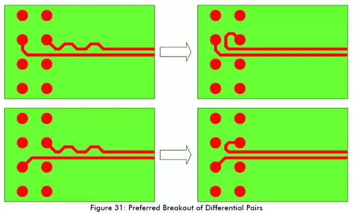
For high-speed differential signal pairs, the two signal lines must ensure strict delay; otherwise, communication may fail. To meet this requirement, serpentine lines can be used to achieve equal length, thus satisfying delay requirements.
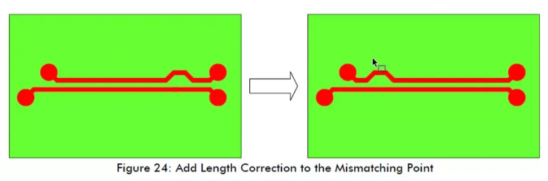
Serpentine lines should generally be arranged at the source of the length discrepancy, not at the far end. Only at the source can we ensure that the positive and negative signals of the differential lines are synchronized during most of the time.
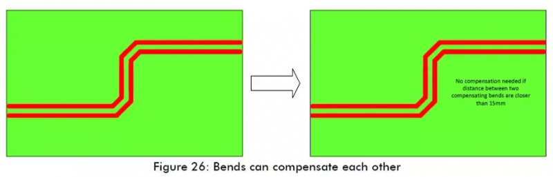
The bending of the routing lines is one of the sources of length discrepancy. For the bending of routing lines, the equal length should be achieved close to the bend (<=15mm).
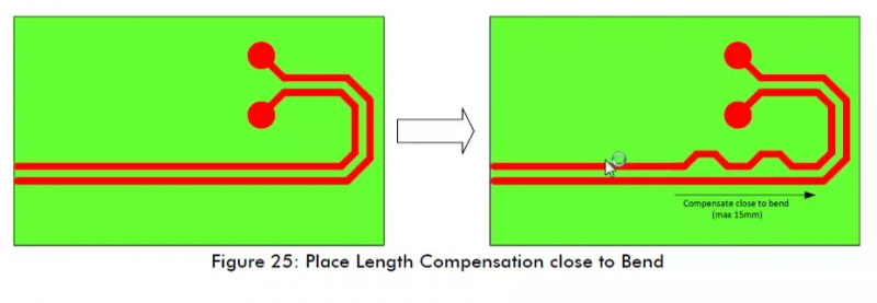
If there are two bent routing lines with a distance of <15mm between them, the length discrepancy between them will compensate for each other, so no further equal length treatment is needed.
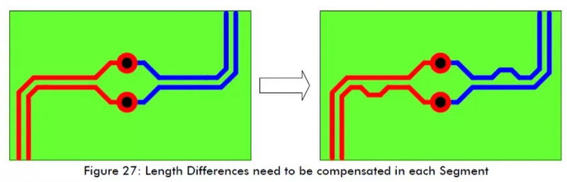
For different parts of high-speed differential signal lines, equal length should be maintained separately. Vias, coupling capacitors, and interface terminals can split high-speed differential signal lines into two parts, so special attention must be paid to ensure they are equal length. Many EDA software only focuses on whether the entire routing has length discrepancy during DRC.
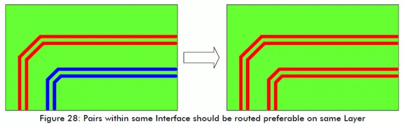
For interfaces such as LVDS display devices, there will be multiple differential pairs, and the timing requirements between the differential pairs are generally very strict, with very small delay requirements. Therefore, for such differential signal pairs, we generally require compensation to be done within the same plane, as the signal transmission speeds are different across different layers.
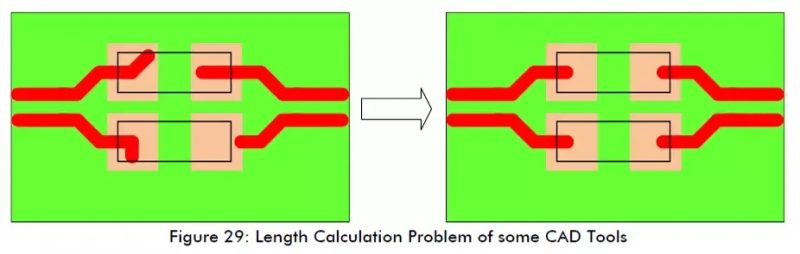
Some EDA software may calculate the routing length by including the routing within the pad, and if length compensation is applied, the final actual result will be a length discrepancy. Therefore, special attention should be paid when using some EDA software.
At all times, if possible, choose symmetric routing to avoid the need for serpentine routing for equal length.
If space allows, try to add a small loop at the source of short differential lines for compensation instead of using serpentine lines for compensation.
Source: Internet
Disclaimer: This article’s copyright belongs to the original author and does not represent the association’s views. The articles pushed by the “Jiangxi Province Electronic Circuit Industry Association” are for sharing purposes only and do not represent the position of this account. If there are copyright issues, please contact us for removal.