PCB grounding is a concern for PCB layout engineers, such as how to effectively plan a grounding system on the board, whether to wire analog, digital, and power grounds separately or together at a single point, and how to eliminate ground loops on the circuit board.
Today, we will mainly discuss PCB grounding design, PCB grounding techniques, and PCB grounding handling.
1. What is Grounding?
Although this question may seem a bit silly, there are differences between different types of grounding. Electrical grounding is a conductive body that serves as a common return path for current from various devices, typically referred to as the 0 potential node, and all other voltages in the system are relative to this node.
Here are different types of grounding nodes:
01、Floating Ground
When a system has no reliable grounding connection, floating ground occurs. Therefore, the voltage at the grounding terminals and conductors is uncertain; unintentional floating ground is considered a system failure (a potential break in the grounding system), but there are also intentional applications that use floating ground.
In low-voltage power supplies and test instruments, isolation transformers are used to isolate low-voltage ground from the main grounding system to enhance safety. By floating the low-voltage side ground, it avoids the grounding current path from the main power supply. If a fault occurs on the low-voltage side, this provides electrical safety.
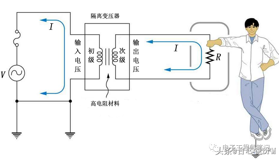 Floating Ground
02、Earth Ground
This is essentially a physical connection to the Earth, serving as a safe return point for dissipating residual current.
03、Chassis Ground (Safety Ground)
Chassis ground (safety ground) is the connection of the safety wire from the AC power supply to the product’s shell or chassis; grounding and chassis grounding serve the same function and are often used interchangeably with the term safety grounding.
In terms of PCB grounding, there is no one-size-fits-all approach. To determine the best way to ground the system, you need to understand how current flows within it. However, there are various methods available, along with some best practices for grounding that apply to most systems.
04、Signal Ground
Signal ground is the reference for any analog or digital signals used in the circuit; most of the time, signal ground is equal to power ground. However, in some cases, signals in the circuit use different isolated grounds to return signal currents, leading to the definition of separate grounds for signals, which can be found in sensitive devices and measuring instruments.
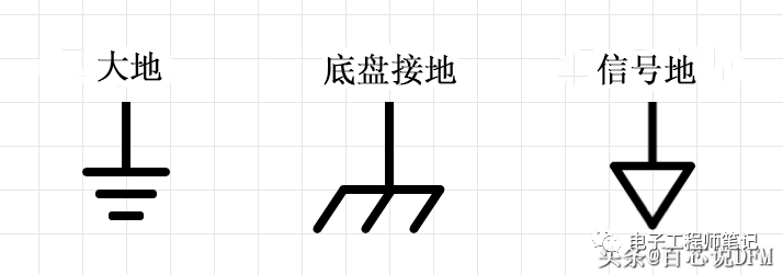
Typical symbols used for grounding in schematics
When dividing the circuit board for analog and digital parts, separated grounds are typically connected beneath or near mixed-signal devices that connect analog and digital tracks. When connecting between the analog and digital ground planes beneath mixed-signal devices, it can run mixed-signal traces with the shortest length and reduce the chances of interference from other analog or digital signals around the device.
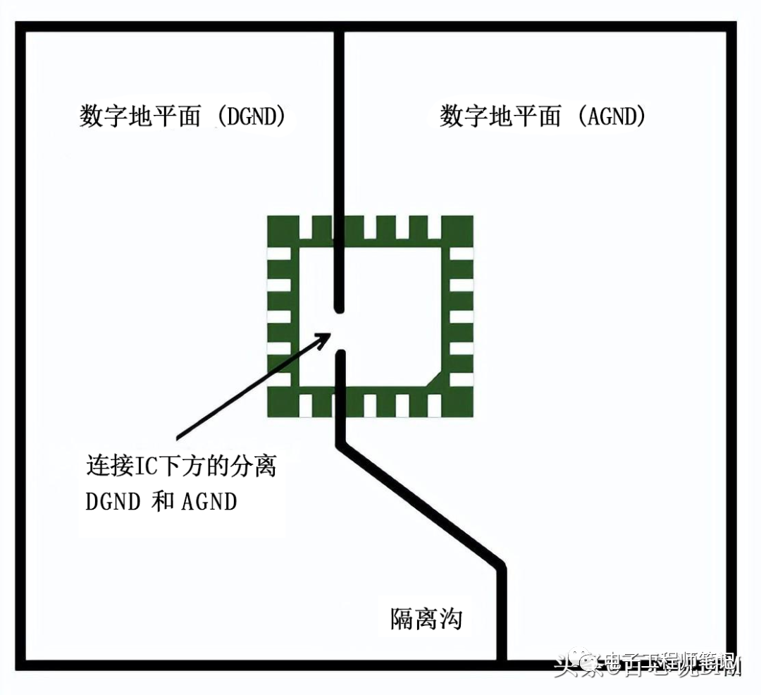
Separate grounding for analog ground and signal ground
05、Virtual Ground
Virtual ground is commonly found in operational amplifiers (Op-Amps). The virtual ground node is not directly connected to the ground (GND) current return path but maintains a match with the ground reference potential. Virtual ground is used to analyze the function of operational amplifiers.
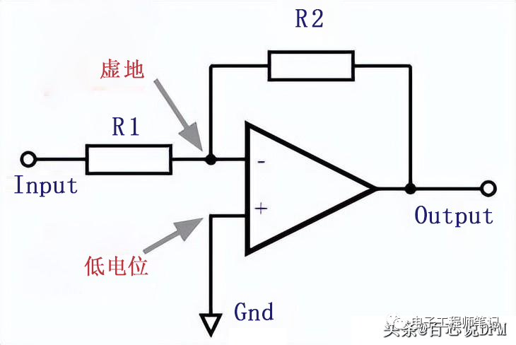 Virtual Ground
By considering the virtual ground potential and assuming that the operational amplifier does not absorb current, the following relationship is obtained.
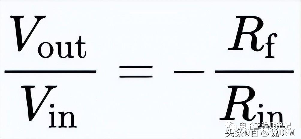
Virtual Ground Calculation Formula
06、AC Ground
AC ground nodes have low impedance DC values, which remain stable even under small disturbances. Due to its DC value, this node cannot serve as a suitable ground, but because it is stable, it can serve as a reference point.
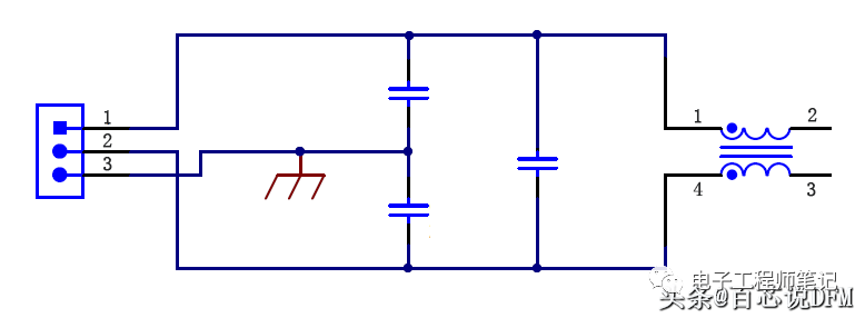
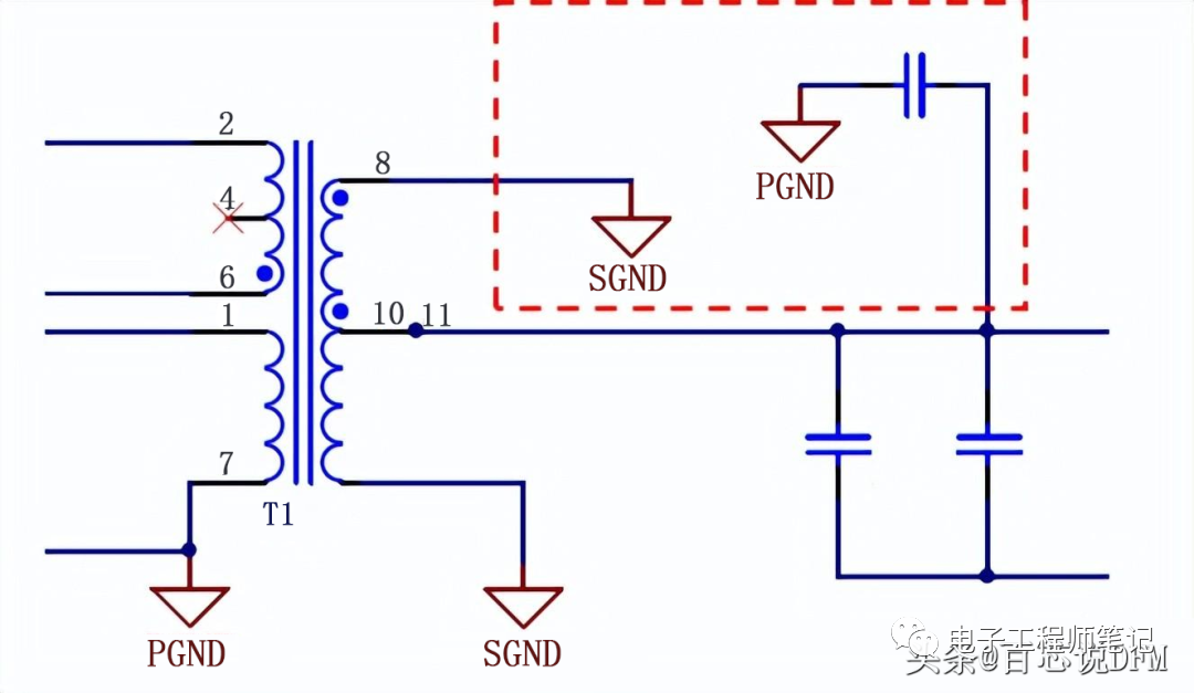
AC grounding is the standard method of introducing power into circuit boards that require grid power and operate at medium to high currents. In the diagram below, we introduce 3-phase AC into the system and use a transformer to step it down to the level required by the circuit board.
The separation between primary ground (PGND) and secondary ground (SGND) in PCB layering means that we now essentially have an isolated power source on the circuit board along with our other important components, which may be high-speed digital or precision analog components.
Input Power Stage Isolation Grounding
07、Chassis Ground
One important point to note in electronic products is that not all systems have chassis grounding (safety grounding). Typically, chassis grounding refers to the metal chassis within the enclosure and is connected to the chassis.
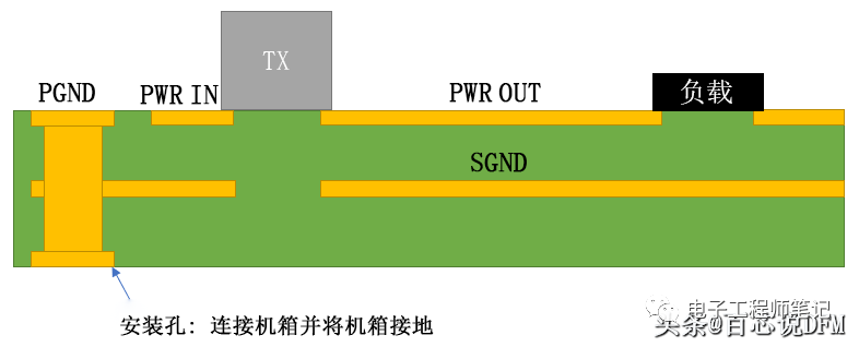
In a 3-wire AC system (live wire, neutral wire, and ground wire) or a 3-wire DC system (DC+, DC common, and ground), chassis grounding is usually connected to the ground at the point where power enters the supply. A part of the system can also be connected to chassis ground to absorb noise or for safety reasons (e.g., ESD protection), as shown in the example below. This arrangement provides common-mode noise filtering for AC or DC input on the 3-wire connection.
The chassis grounding in the schematic below is directly connected to the circuit board and has low-inductance grounding contacts with the enclosure. Note that pin 3 on the connector is the ground wire.
Chassis Ground
The chassis grounding connection provides three functions:
Since the chassis is now set as the global 0 V reference potential, the chassis now acts as a Faraday cage and provides broadband shielding.
It provides a safety function to dissipate parasitic currents (ESD, short circuits, or noise) back to the ground.
It can provide a low-impedance receiver for common-mode noise on this input EMI filter without the need to place ferrite or large choke coils on the board.
08、Multi-Grounding
Multi-grounding usually occurs when wiring between two devices, and the cable may have some shielding connected to the ground wire at each end.
Care must be taken here, as there may be a DC potential difference between the two grounding connections, which can be around 10 V when measured in the laboratory. If grounding bridging occurs (e.g., using shielding along the shielded cable), grounding offset may cause large DC currents to flow through the cable.
Multi-Grounding
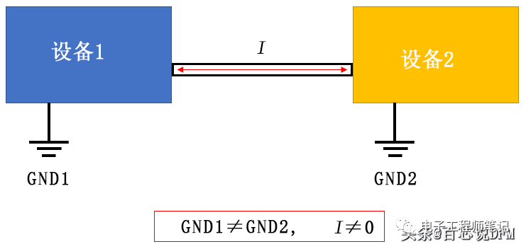
2. Not All Grounds are 0V
Floating conductors or conductors in the system referencing different power sources may not have the same 0 V potential. In other words, two different devices have two grounding participants but are connected to the same reference; if you measure the potential between them, the measured voltage is a non-zero voltage.
In power systems, care must be taken on how to use capacitive grounding to ensure that grounding references remain consistent. Y-capacitance is most suitable; you need to eliminate the DC offset between planes while providing current isolation and high-frequency EMI filtering.
PCB Grounding Circuit
When two devices reference the same conductor as a grounding connection, the following situation may occur. If you measure the potential difference across a long conductor (e.g., using a multimeter), it may not be 0, indicating that some current is driving along the conductor. This potential difference along the ground or between two grounding connections is referred to as “ground offset.”
3. PCB Grounding Design
01、Ground Line
All components connected to the ground are connected together through a common trace, which is common in older PCBs and simple PCBs.
 Ground Line
02、Common Ground Plane
The common ground plane is the most common practice in PCB design. The free space on the PCB not utilized by traces or components is covered from the ground. The common ground plane significantly improves the thermal characteristics of the PCB and helps reduce electromagnetic interference (EMI).
03、Dedicated Ground Layer
The dedicated ground layer is used in multilayer PCBs, where components are connected to the ground layer through grounding vias. It can be found in densely packed complex PCBs with three or more layers.
Dedicated Ground Layer
04、Power System Grounding
In power system installations, all grounding connections are connected to a grounding bus. This bus connects to a grounding conductor, which is connected to a grounding rod or grounding grid.
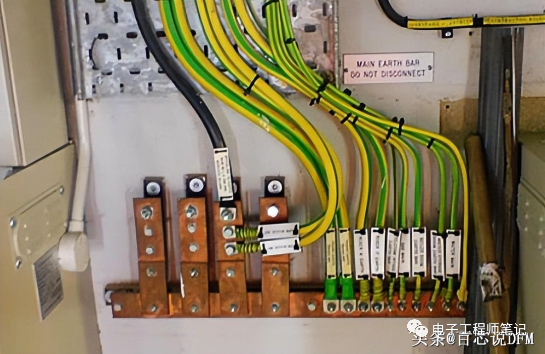 Power System Grounding
The grounding bus collects all grounding wires from all devices into a common point. The grounding resistance at this point should be less than 5 ohms to provide better grounding, using high-spec wire to connect the grounding bus to the grounding device (grounding rod and grounding grid).
05、Equipotential Grounding or Grounding
Equipotential grounding means that every conductive element in the protected area should have the same grounding potential, achieved through electrical connections between the equipment chassis, metal pipes, and all grounding devices.
Equipotential ensures that there is no significant potential difference between any conductive parts in the area, preventing electric shock during faults.
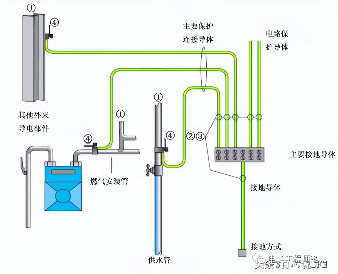 Equipotential Grounding or Grounding
4. PCB Grounding Techniques
01、PCB All Connections Complete
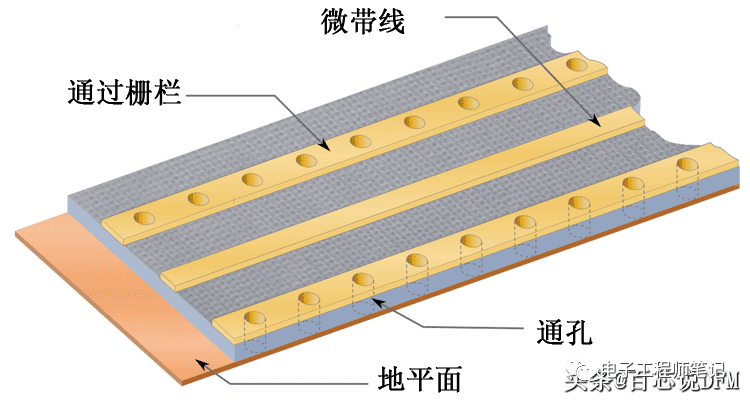
No open spaces should exist on the PCB layout. If your board has an open space, it should be filled with copper and vias to connect to the ground layer, creating a structured path for all signals on the PCB to effectively reach the ground.
02、Ground Layer
Using a ground layer is one of the most common techniques among many PCB designers. Ground layers are typically made of copper and cover all areas of the PCB that do not have components or traces. Some rules apply to ground layers depending on the number of layers on the circuit board. For example, if the circuit board has two layers, the rule states that the ground layer should be on the bottom layer, with traces and components on the top layer.
When placing a ground layer, ensure that it does not form a conductive material loop. This loop increases the sensitivity of the ground layer to electromagnetic interference (EMI). When an external magnetic field interacts with a conductive loop, it acts as an inductor, generating current known as a ground loop. Ground loops can interfere with other circuits that generate electrical noise.
When a ground layer is placed beneath the entire bottom layer and all electrical components are removed, a conductive loop may form. Ensure that traces are as short as possible and place the ground layer beneath them to prevent ringing. Additionally, the layout of traces and components can be adjusted to avoid creating conductive loops.
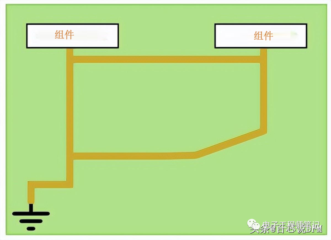
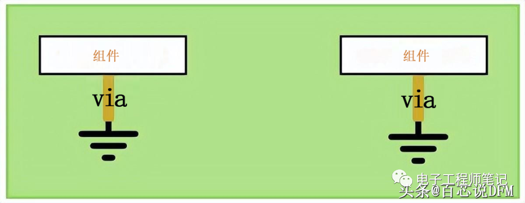
Each component must be individually connected to a solid ground layer to avoid ground loops.
Ground Loop Formed by Two Traces Connected to the Ground Layer
When using chassis grounding, you can avoid ground loops by placing a gap in the grounded part connected to the chassis, as shown below. The use of capacitors provides an AC grounding point. This is an ideal situation for electrical devices that need to use wall power and require a direct return to the ground.
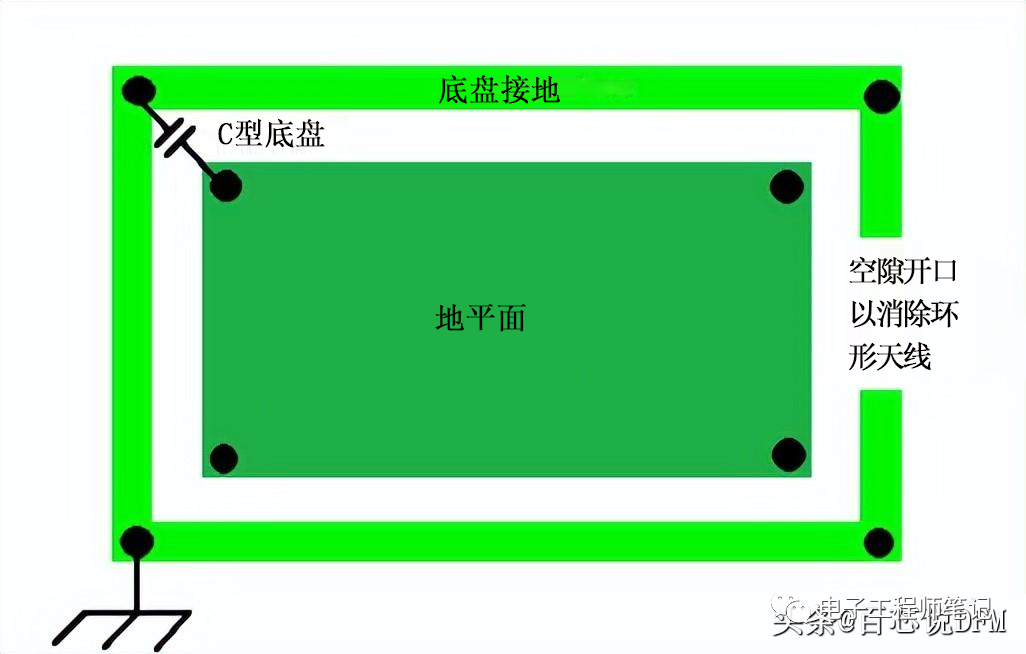
Eliminating Ground Loop Antennas
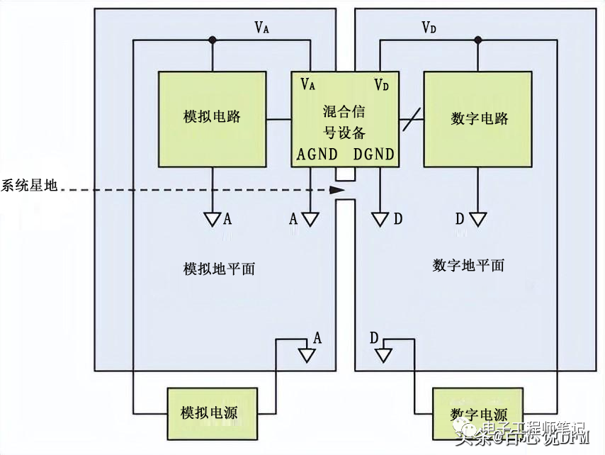
03、Arrangement of Analog and Digital Components
Components should be arranged on the signal layer close to ground to shorten the return path and couple traces to ground. If the PCB contains both analog and digital components, care must be taken when placing grounding connections. The analog and digital parts of the circuit board should be physically separated, but they still need to connect to the power return path.
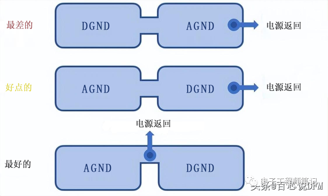
Mixed Signal Grounding Connections
Some may suggest completely separating digital ground and analog ground and then connecting them with ferrite beads, but this may create more EMI and noise problems than it resolves, especially when operating at very high frequencies.
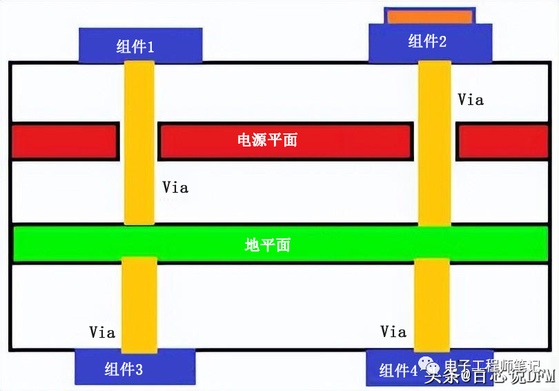
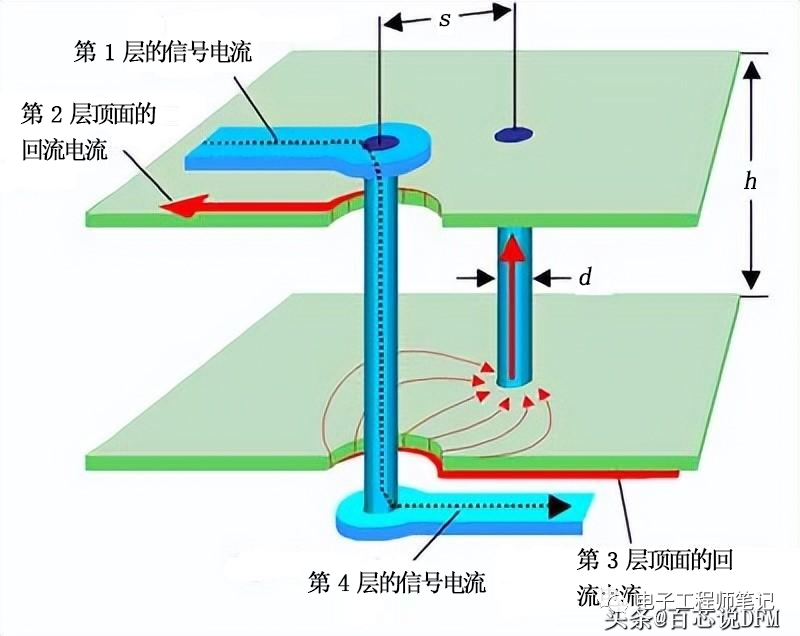
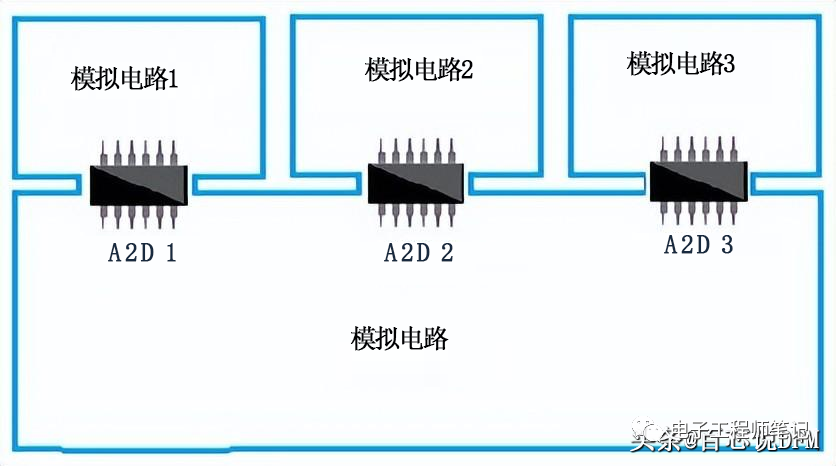
A good way to connect these parts is to place the power return path between the two planes so that the return current of either part does not enter the other plane. It is important to note that no traces should be routed over the gap between two grounding layers, as this would create long current return paths that are highly susceptible to EMI. The space between grounding layers can be used to place mixed-signal components such as ADCs.
04、Ground Layer Vias
If there are ground layers on both sides of the PCB, they will connect through vias at many different locations on the board. These vias are holes that pass through the circuit board and connect the two sides, allowing access to the ground layer from anywhere that a via can be inserted.
Using vias can help you avoid ground loops. They connect components directly to the ground point, which is connected to all other ground points in the circuit through low impedance, while also helping to shorten the length of the return loop.
Ground Layer Vias
The ground plane typically resonates at specific wavelengths of the frequency of current flowing into it. You should place vias around the ground layer at precise intervals to avoid ground layer resonance. Tentative vias are an important aspect of PCB boards, as they help transfer heat to the other side of the board through vias, aiding in cooling hot-running components.
In PCB layouts without vias, you can drill a few holes with a small drill press and then pass copper through the holes and solder to achieve connections on both sides.
05、Decoupling
Decoupling is the process of implementing LC networks next to integrated circuit chips to provide transient switching currents. Power pins for integrated circuit chips are installed to connect them to external power. Additionally, grounding pins are included to connect them to the PCB ground layer.
Decoupling capacitors should be placed between the power pins and the ground plane to eliminate oscillations caused by voltages provided in the chip.
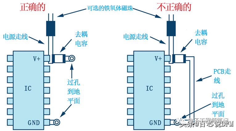
Correct and Incorrect Placement of High-Frequency Decoupling
Decoupling capacitors are vital for improving and enhancing the functionality of the PCB. Capacitors are designed to store charge, so decoupling capacitors in the PCB act as charge storage devices.
Thus, if an IC requires more charge, the decoupling capacitor provides charge to the IC through a low-inductance path. Besides enhancing PCB functionality, decoupling capacitors also effectively reduce noise generated on multilayer planes. Additionally, decoupling capacitors reduce EMI.
06、All Connectors in PCB Should be Grounded
In connectors, all signal lines must run in parallel. Therefore, you must use grounding pins to separate connectors.
Each circuit board may need multiple connector pins connected to ground. Only one pin may lead to impedance mismatch issues, resulting in oscillations. If the impedances of two conductive connections do not match, the current flowing between them may bounce back and forth, and these oscillations will alter the system’s performance and cause it to not work as expected.
The contact resistance of each pin in the connector is very low, but it may increase over time. Therefore, it is best to use multiple grounding pins. Approximately 30% to 40% of the pins in PCB connectors should be grounding pins.
Connectors have different pitches and can have various numbers of pin rows; the pins of the connectors can also run parallel to the PCB surface or at right angles to it.
07、Always Provide a Common Ground Point
Whether it is a single-layer PCB or a multilayer PCB, a point is required to connect all ground points together. This could be a metal frame on the chassis or a dedicated ground layer on the PCB, which is often referred to as star grounding.
08、Minimize Series Vias
Ensure to minimize series vias on the grounding path, but rather send the component grounding directly to the dedicated ground layer.
The more vias added to the circuit board, the greater the impedance that must be dealt with, which is particularly important for fast transient currents that can turn impedance paths into voltage differentials.
09、Design Grounding Before Routing
Before doing any routing, it is essential to properly design the ground, which is the foundation for the entire routing process.
10、Determine the Direction of Current on the PCB
Many designers only consider where their signals are transmitted, but every signal has a return path through the ground. The sending and returning paths of the signals will have the same current, affecting power stability and ground bounce.
You can use Kirchhoff’s current law to understand how current will flow through your circuit.
 Determine the Direction of Current on the PCB
11、Ground Layers in Stacks
In multilayer PCBs, the arrangement of power, signal, and ground layers in the stack has a significant impact on signal integrity and will affect routing strategies.
It is important to keep ground layers close to signal layers to minimize the return path of currents. In a 4-layer board, power and ground layers are typically located in the inner layers, while signal traces and components are located in the outer two layers.
12、Plan for Dynamic Differences Between Ground Planes
When sending grounding connections between the boards of multilayer PCBs, always plan for dynamic changes. This is especially true in applications requiring long-distance cables.
For these cases, you can use low-voltage differential signals, optical isolators, and common-mode chokes to control variations.
13、Pay Attention to Wiring Distinctions in Mixed Signals
The analog portion of the circuit board needs to be separated, including ADCs and DACs.
When designing the “layout” of the PCB, it is essential to isolate these areas. The grounding of the ADC can connect to a common ground point, and digital signals can be transmitted to other parts of the PCB through this common ground point.
Attention to Mixed Signal Plane Planning
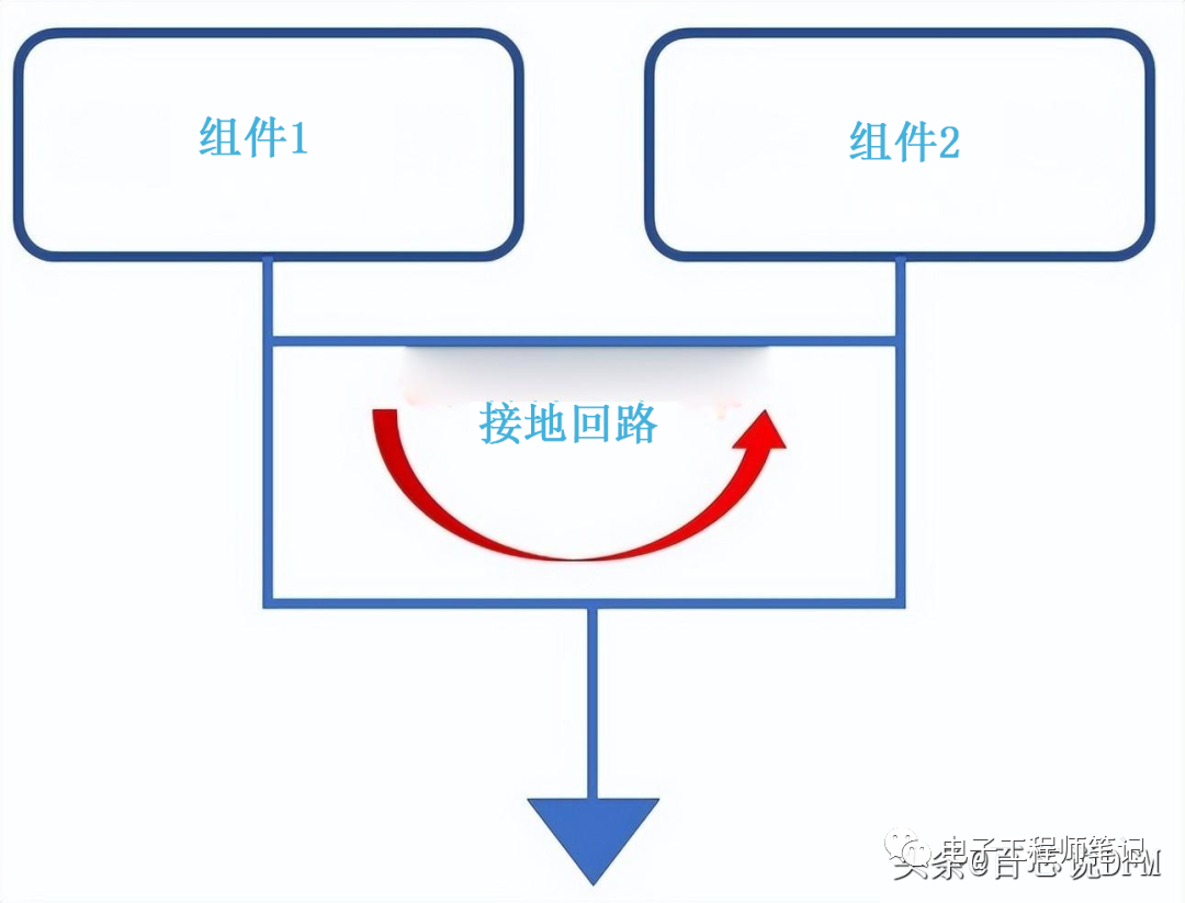
14、Avoid Ground Loops
By experience, the term “ground loop” can refer to any situation where the system is affected by differences in ground potential. A typical example is when two modules are connected by a long cable, and the return current in the cable causes the ground voltage of one module to be significantly higher than that of the other module. However, here it specifically refers to ground loops. For example:
Ground Loop
If you must use separate PCB traces for a large number of grounding connections, it can be easy to create loops as shown in the image above.
The existence of ground planes does not mean that ground loops cannot be created, as CAD programs do not prevent you from drawing traces between grounding points. However, if you always use vias or through-holes for grounding connections, the problem should largely disappear: by placing vias on the plane, you can connect directly from components to the grounding point, which is connected to all other points in the grounding circuit through low impedance.
Avoid Ground Loops
In PCB layouts, it is important to correctly place components. Connections for splitting ground layers can be made directly beneath the components to avoid ground loops.
 Avoid Ground Loops
In PCB layouts with multiple subsystems, mixed signal components can be carefully arranged to connect board partitions beneath the components to avoid ground loops.
The above is about PCB grounding techniques, and I hope everyone can support it.