In recent years, with the rapid development of the new energy vehicle industry, the three electric systems related to new energy vehicles—batteries, electric drives, and electronic control systems—are continuously being upgraded. To improve the range of new energy vehicles, the three electric systems are constantly being updated, especially with the main goal of increasing the conversion efficiency of the electric drive system. In traditional main drive inverters for new energy vehicles, power modules use copper-clad ceramic substrates with high thermal conductivity and electrical insulation properties as carriers for inverter power chips, and then adopt frame and injection molding for overall packaging, achieving electrical connections through bonding wires (as shown in Figure 1). These two packaging methods impose significant limitations on the overall heat dissipation and electrical performance of the module, and the bonding wire method leads to considerable parasitic inductance in the module’s commutation and control circuits, ultimately resulting in lower conversion efficiency.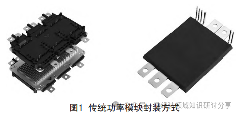 Currently, the power density and integration of power modules are continuously increasing, coupled with stringent thermal management requirements. PCB embedded packaging technology has become the preferred solution due to its numerous advantages. Specifically: (1) High integration: Embedded components (such as capacitors, SiC chips, etc.) are placed directly within the PCB, reducing the demand for surface space, allowing more functions to be integrated within a smaller area; (2) Compact size and lightweight: By embedding active and passive components into the multilayer structure of the PCB, a more compact circuit design can be achieved, thereby reducing the size and weight of the final product; (3) Enhanced electrical performance: The three-dimensional stacking of components shortens signal transmission paths, reduces parasitic inductance and capacitance, which helps to minimize signal interference and electromagnetic interference (EMI), thus improving signal integrity; (4) Thermal management: By using copper foil as a substrate or embedding heat dissipation channels within the multilayer, thermal energy can be managed more effectively, especially in high-power applications. Although FR4 material has low thermal conductivity, careful design and the use of ceramic substrates can optimize thermal paths and reduce thermal resistance; (5) Design flexibility: Allows for the arrangement of control circuits and power circuits on different layers of the product, simplifying the design process while providing more design freedom, facilitating rapid iteration and customization. PCB embedded packaging has the potential to become the future development direction of power modules; (6) Reliability: Embedded designs reduce external connection points, lowering the risk of failures due to mechanical stress and improving long-term reliability. These advantages determine that PCB embedded packaging technology will be the future trend in power module development.1 PCB Embedded Packaging Solutions1.1 PCB Product Stacking Scheme The sintered chip AMB module is embedded within the PCB using a pressing method, and interlayer circuit connectivity and chip commutation circuit and gate circuit control are achieved through laser blind hole technology and wiring layer routing (as shown in Figure 2).
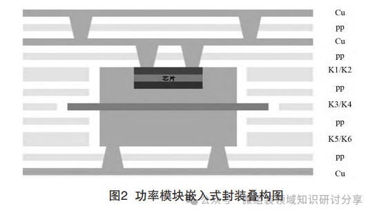 The source and gate above the chip are controlled through laser holes and wiring layers, achieving electrical and thermal isolation through the copper base and ceramic of the AMB module. The wiring layer above the AMB module implements related circuit functions, and the heat generated during module operation is conducted through the densely packed laser holes on the bottom surface to the external heat sink, achieving module cooling.2 Key Processes of Embedded Packaging Currently, there are two main methods for sintering SiC chips. The first method involves directly sintering the SiC chip onto the surface of the active metal soldered AMB using silver sintering. This method results in the chip surface being higher than the copper base surface after sintering, making the SiC chip prone to cracking during the pressing process, which is detrimental to processing. The second method involves grooving the copper base on the active metal soldered AMB surface and then sintering the SiC chip using silver sintering within the groove. This method results in the sintered chip being flush with the copper base surface, which is more favorable for the PCB embedded packaging process. This study primarily focuses on implementing the second method.2.1 Research on AMB Grooving Method2.1.1 Chemical Etching The conventional manufacturing method uses chemical etching to create grooves; however, this process suffers from insufficient bottom flatness, leading to stress concentration points after chip sintering, which can cause SiC chip fractures after embedded packaging (as shown in Figure 3).
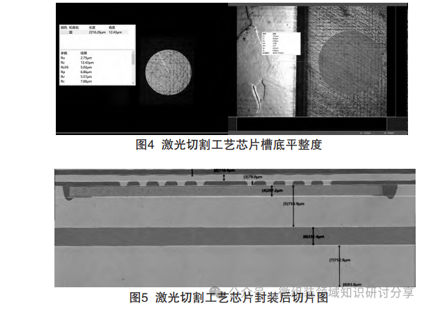
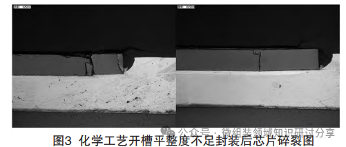 The chemical etching process is influenced by parameters such as the etching factor. If the bottom flatness is acceptable, the etching groove dimensions need to be increased, which poses a significant challenge to the consistency of chip sintering. A process is needed to address the flatness issue of the sintering groove bottom.2.1.2 Laser Etching Research has shown that using laser cutting as a physical process can meet the requirement for flatness of the chip groove bottom. Using picosecond laser equipment, laser grooving is performed on the copper base above the AMB module. By setting parameters such as laser spot diameter, beam center spacing, energy power for different segments, number of layers, and number of cycles, different experimental schemes are tested. Five test schemes are set with beam center spacings of 4, 5, 6, 7, and 8 μm, with consistent laser energy power, and corresponding cycle counts are selected (see Table 1), ultimately producing grooves that meet the flatness requirements for chip sintering. As shown in Figure 4, the roughness Sa of the chip sintering groove produced by laser cutting can reach 2~5 μm.
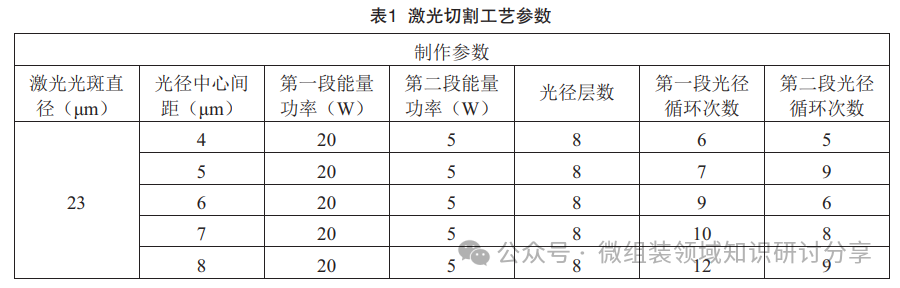 The chip grooves produced by laser cutting, after chip sintering, showed no signs of chip fracture failure during slice analysis of the AMB module after PCB embedded packaging (as shown in Figure 5).
 2.2 AMB Module Pressing Scheme The AMB structure consists of a copper base + ceramic layer + copper base sintered together using active soldering technology, achieving electrical insulation. The AMB module is a special-shaped module, and to ensure safe creepage distance, the ceramic layer is usually larger than the copper base size. By creating patterns on the AMB module copper base, corresponding electrical functions are realized, and the SiC chip is sintered into the AMB module copper base using a recessed sintering method, which meets the current-carrying requirements of the power chip and the heat dissipation requirements of the power module. However, the AMB module has the common disadvantage of ceramic products, which is insufficient rigidity, leading to a risk of ceramic fracture during PAB embedded packaging (as shown in Figure 6).
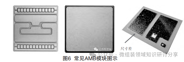 Due to the risk of ceramic fracture in the AMB module, when performing PCB embedded packaging, it is necessary to use FR4 board fixtures corresponding to the shape of the AMB module for pressing. During the pressing process, adjustments and monitoring of the pressing stack and parameters, as well as the size of the AMB module ceramic and copper base, are required to ensure the integrity of the AMB module. Tests have shown that the size difference between the AMB module ceramic and copper base is the main factor leading to ceramic fractures after embedded packaging. Adjusting the size difference can resolve the ceramic fracture issue. Using the same pressing stack and parameters, different ceramic and copper base size differences were tested. Scheme one used an AMB module ceramic edge size 4 mm larger than the copper base size, while scheme two used an AMB module ceramic edge size 0.7 mm larger than the copper base size. After embedded packaging, scheme one showed ceramic edge fractures, while scheme two showed no fractures (as shown in Figure 7).
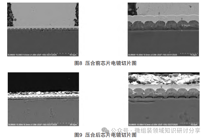
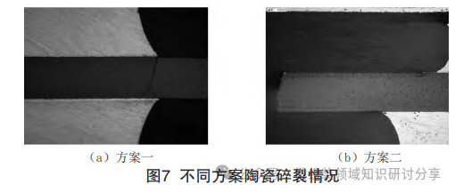 By reducing the AMB module ceramic edge size from 4 mm to 0.7 mm, the torque and stress on the ceramic were reduced, and the issue of ceramic edge fractures was resolved. Simultaneously, slice and electron microscope analysis of the SiC chip above the AMB module confirmed that there was no damage to the chip after the PCB pressing process, and the chip’s electrical performance tests showed that the chip functioned normally (as shown in Figure 8).
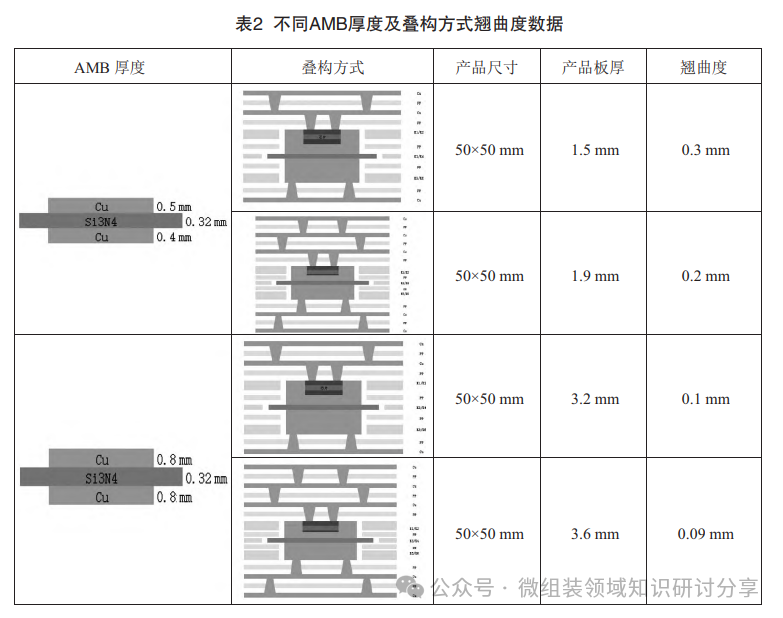
 2.3 Impact of Embedded Stacking on Warpage For conventional PCB products, the product stacking is usually symmetrical; asymmetrical structures can lead to warpage, affecting product usability and reliability. To achieve high heat dissipation requirements, embedded power modules have implemented thermal and electrical separation, with electrical performance realized through the wiring layer above the module, and the number of wiring layers determined by the number of chips in the module, while the bottom of the module directly connects to the heat sink, thus the optimal solution is to avoid stacking at the bottom, allowing the copper base of the AMB module to connect directly to the heat sink for optimal heat dissipation. For this stacking method, warpage is inevitable after PCB product fabrication, thus it is necessary to optimize the pressing stack to ensure that the product meets warpage standards without affecting usability. To verify the warpage of products after embedded packaging with different stacking methods and AMB module thicknesses, two experimental schemes were designed. Data on warpage under different AMB thicknesses and stacking methods were collected. Scheme one: AMB module with copper base thickness of 0.5 mm + ceramic thickness of 0.32 mm + copper base thickness of 0.4 mm, using 1~2 and 2~3 pressing stacking methods, with a single product size of 50 mm*50 mm. Scheme two: AMB module with copper base thickness of 0.8 mm + ceramic thickness of 0.32 mm + copper base thickness of 0.8 mm, using 1~2 and 2~3 pressing stacking methods, with a single product size of 50 mm*50 mm. The warpage measurements after pressing for both schemes are shown in Table 2. From the data in Table 2, it can be seen that as the AMB thickness increases, the warpage of the PCB product after embedded packaging decreases. Changing the stacking method from 1~2 to 2~3 also shows a trend of reduced warpage. Therefore, by adjusting the AMB thickness and pressing stacking method, the issue of asymmetrical pressing warpage can be improved. Additionally, using materials with different CTE values, adjusting residual copper rates, and modifying pressing process parameters can significantly improve the warpage issues of asymmetrical embedded PCB packaging.2.4 Chip Laser Hole Process Parameters The embedded PCB of the power module achieves electrical performance connectivity through the wiring layer, with the upper wiring of the AMB module connected to the wiring layer via laser blind holes and electroplated filled holes, realizing the functionality of different poles of the SiC chip. The laser drilling process is a mature processing technology for conventional PCB products, typically involving copper pads with a thickness of about 35 μm.
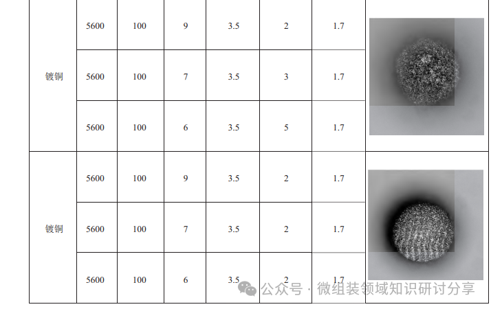
 For SiC chips in power modules, unlike conventional PCB products, the surface treatment of the chip varies, leading to significant differences in the thickness of surface coatings. Currently, the mainstream surface coatings for SiC chips in the market are nickel-palladium-gold and copper plating. The nickel-palladium-gold chip surface coating consists of: palladium layer 0.1 μm, nickel layer 4 μm, gold layer 0.05 μm, while the copper-plated chip surface coating is approximately 15 μm thick. Different surface coatings require different parameters during laser drilling, and improper parameters can lead to laser penetration of the chip surface, causing chip failure. To verify the compatibility of different surface-treated chips with the laser drilling process, four comparative experiments were designed, using different laser parameters for validation, to check whether the surface coating state and functionality of chips with different surface treatments would be damaged after laser drilling with different parameters. Experiment one: A chip with a nickel-palladium-gold coating, with thicknesses of palladium layer 0.1 μm, nickel layer 4 μm, gold layer 0.05 μm, using the same laser equipment, thus output and frequency parameters were consistent at 5600 and 100 Hz, with an energy of 3.5 mJ, pulse width of 3.5 μs, and laser counts of 2+3+5. Experiment two: A chip with a nickel-palladium-gold coating, with thicknesses of palladium layer 0.1 μm, nickel layer 4 μm, gold layer 0.05 μm, using the same laser equipment, thus output and frequency parameters were consistent at 5600 and 100 Hz, with an energy of 3.5 mJ, pulse width of 3.5 μs, and laser counts of 2+2+2. Experiment three: A chip with a copper layer, with a thickness of 15 μm, using the same laser equipment, thus output and frequency parameters were consistent at 5600 and 100 Hz, with an energy of 3.5 mJ, pulse width of 3.5 μs, and laser counts of 2+3+5. Experiment four: A chip with a copper layer, with a thickness of 15 μm, using the same laser equipment, thus output and frequency parameters were consistent at 5600 and 100 Hz, with an energy of 3.5 mJ, pulse width of 3.5 μs, and laser counts of 2+2+2. After completing the four experimental tests, the experimental data is shown in Table 3. From the parameters in Table 3, it can be seen that when laser energy is inappropriate, the nickel-palladium-gold coating on the chip can be penetrated by high-energy lasers, leading to chip failure. By adjusting laser parameters such as energy, pulse width, number of emissions, and aperture, suitable laser parameters can be established to create laser holes above the nickel-palladium-gold coating on the chip. Additionally, from the comparison of parameters in Table 3, it can be seen that copper-coated chips can withstand greater energy than nickel-palladium-gold coated chips, providing a larger processing window and higher yield after laser drilling. Currently, nickel-palladium-gold coated chips are more mainstream in the market, while copper-coated chips require an additional copper plating process. Therefore, when producing, considering the appropriate coating chip and suitable process parameters is key to ensuring product quality. After completing the laser hole creation above the chip, electroplated copper is used to fill the holes, and through these electroplated copper pillars, the electrical control performance of the chip is realized, while the laser blind holes achieve interconnection of the wiring layer, realizing the entire module’s functionality (as shown in Figure 9).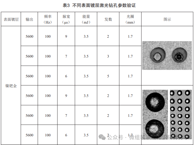
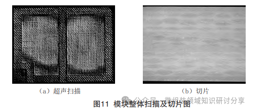
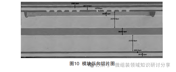 3 Embedded Module Testing3.1 Module Related Testing After the module is completed, relevant performance tests are conducted, including ultrasonic scanning and physical slice analysis of the module to confirm that there are no voids caused by insufficient adhesive filling (as shown in Figure 10).
 4 Conclusion This article introduces a PCB embedded power module manufacturing process. By adopting the advantages of traditional PCBs, the integration of power modules with them can significantly enhance the performance and reliability of power modules. Moreover, PCB technology is currently very mature, making this process a promising packaging technology. PCB embedded power modules far exceed traditional packaging in terms of unit power cost, power density, conversion efficiency, and reliability, and are expected to become a new direction in the future automotive power electronics industry.Thanks to Teacher Li Longfei from Shenzhen Mingyang Circuit for the article.If interested, you can join the micro-assembly group for power devices and hybrid circuits.