
PCB design is both a science and an art. There are many technical specifications related to trace width, layer stacking, schematics, etc. However, when it comes to the artistic aspects of component placement in PCB design, the issue becomes interesting.
In fact, there are very few restrictions on component placement, and there are no “absolutely correct” specifications. This allows beginners to arrange components on the circuit board as if they were in a “middle school phase,” aspiring towards personal ambition and creativity. How you place them entirely depends on you and your design philosophy.
But this does not mean you can do whatever you want. The design in the computer ultimately has to materialize into something usable. Therefore, the following ten tips for PCB component placement can guide electronic beginners through the initial stages of electronic design smoothly.
Why is Component Placement So Important?
There is an old saying (unknown origin): 90% of PCB design is in component layout, and 10% is in routing. This is indeed a profound truth. Taking the time to carefully place components can yield exponential results and improve the electrical characteristics of the PCB. What happens if you just randomly place components on the circuit board?
-
Time Wasted: There is a high chance that during routing, you will find that there isn’t enough space in some areas, and you may need to start the entire routing process over.
-
Circuit Board Doesn’t Work: You might think that once the components are placed and all leads are routed, everything is fine. You send the design files to the PCB manufacturer and wait a few days for the new circuit board. Just as you are about to joyfully solder the circuit, reality hits hard when you find out that some components cannot be soldered at all (either due to incorrect packaging or conflicts).
-
Aesthetic Ruined: We must admit that even as humble engineers, we still recognize the pursuit of aesthetics in symmetry and detail. A circuit board where the components were placed without care will only lead to more frustration during soldering and debugging, leaving you with nothing but a sense of defeat.
If you encounter a nitpicker, they might argue that there are no strict rules for component placement. The same circuit diagram can have 100 electronic engineers proposing 1000 different wiring schemes. This is why designing a circuit board is often seen as an artistic creation process.
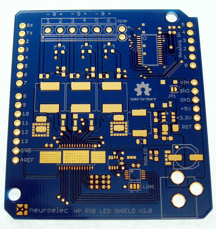
▲ An elegant, artistically designed circuit board easily attracts attention. Symmetrical, tidy, and beautifully placed components!
If you always want to clarify right and wrong, here’s a small trick to help you judge whether your PCB component placement is appropriate.
After placing the components, use the auto-routing feature in your PCB design software (like Autodesk EAGLE) to route the connections. If the final circuit connectivity rate is below 85%, it indicates that you need to spend more time optimizing the component placement.
Now, let’s talk more about practical tips for component placement.
Tip: Understand the Physical Limitations of the PCB
Before placing components, you need to know the locations of mounting holes, edge connectors, and the mechanical size limitations of the PCB. Why?
Because these factors affect the size and shape of your PCB. I’ve seen a design where the PCB couldn’t fit into the designated area, necessitating a redesign.
To avoid making such mistakes, intentionally set a clearance area around those mechanical constraints (mounting holes, PCB outline, etc.) so you can confidently create within the allowable range.
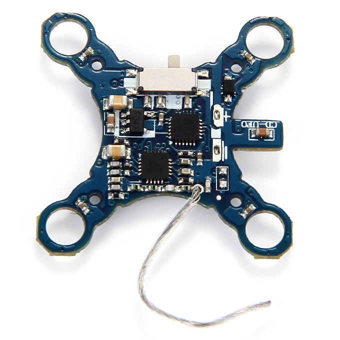
▲ Quadcopters or other flexible wearable circuits often require interesting PCB designs. This is the appearance design of a signal receiving circuit used in a mini quadcopter.
Tip: Understand the PCB Manufacturing Process
Similarly, before placing circuit components, it’s best to clarify several key pieces of information from the circuit manufacturer:
-
Assembly processes and testing procedures for the circuit;
-
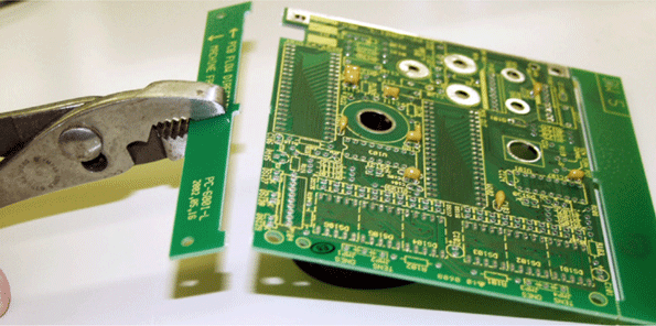
Whether space needs to be reserved for PCB V-groove cutting;
-
Soldering process for components: wave soldering, selective soldering, or hand soldering?
The PCB manufacturing process will affect the required spacing between components. Additionally, if your PCB will be soldered on a production line in the future, you need to leave extra space (greater than 20 mil) at the edges of the PCB for securing it to the conveyor belt. An additional fixture on the PCB is removed after soldering.
Tip: Leave Breathing Space for Integrated Chips
Note that the “breathing” mentioned here is not about air; you will understand what it is after reading below.
When arranging any components, always leave at least 350 mil of space between them, and for chips with many pins, the space needs to be larger. Why?
Modern chips have more and more pins, becoming increasingly dense. If integrated chips are placed too closely, there is a high chance that their leads cannot be easily routed.
Typically, the later you get into routing, the harder it becomes. Sometimes it takes a toll on your patience, and you may find yourself in a situation where you feel helpless. (If only you had known this earlier.)
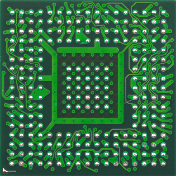
▲ See, this BGA packaged chip has densely packed pins. If you don’t leave enough space around it, you will have a tough time routing.
Tip: Align the Direction of Same Components
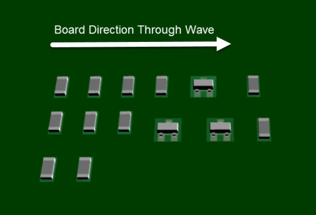
For identical components, try to align them in the same direction. Are you a perfectionist? This is mainly to facilitate the assembly, inspection, and testing of the PCB later, especially for surface-mounted devices during wave soldering, where the PCB passes through a melting solder wave at a constant speed. Uniformly placed components will heat evenly, ensuring high consistency in solder joints.
The example below shows that uniformly placed components are suitable for a constant-speed wave soldering process.
▲ Example of uniformly placed components; the consistent direction is suitable for the constant-speed wave soldering process.
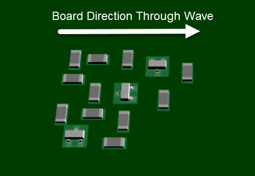
If you place components in a messy manner as shown below, the quality of solder pads during wave soldering will vary for different components, especially when some small components are located between larger ones, creating a “shadow” effect that may lead to poor soldering of the smaller components.
▲ Example of messy component placement: components with different orientations may lead to poor solder joints during wave soldering.
Tip: Reduce Lead Crossings
By adjusting the position and direction of components, you can reduce lead crossings. How?
Many PCB design software tools now offer a feature that displays the connection relationships between unconnected pins.
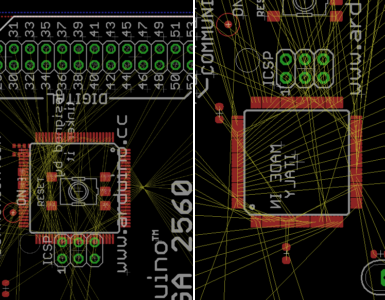
For example, the following image shows all the pin connection relationships in the schematic, represented by thin gray lines (these lines are called ratsnest).
▲ PCB interface showing ratsnest connections.
By changing the position and direction of components, you can minimize lead crossings, saving a lot of effort for the subsequent routing.
Tip: Place Edge Components First
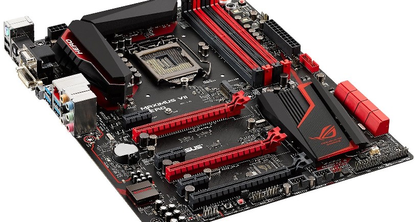
For components that cannot be freely moved due to mechanical limitations, such as external connectors, switches, USB ports, etc., they should be placed first. Why?
These components are often positioned during the overall mechanical design of the system and cannot be changed. Once these components are placed, you have a glorious starting point for arranging the remaining components. After placing the edge components, the rest is your moment to unleash your imagination and creativity.
▲ The position of peripheral interface components on a computer motherboard is closely related to the chassis design, and their positions need to be predetermined.
Tip: Avoid Conflicts Between Components
Absolutely avoid overlapping pads of components or overlapping edges of components just to route on a small PCB. It’s best to maintain a distance of 40 mil (1mm) between all components. Are you afraid of crowding?
The most important reason is to avoid short circuits between pads during the subsequent PCB fabrication process. Remember, tight placement also makes routing more difficult.
Similarly, when placing vias, avoid excessive density. These small holes may later expose copper, causing circuit shorts.
Tip: Keep Components on the Same Side
If you are designing a two-layer PCB, the most common advice is to place components on the same side. Why?
If components are not placed on the same side of the PCB, it will complicate the PCB fabrication process later. Here’s why: typically, components on the PCB are placed using automated machines, and if the components are on one side, the PCB production process only needs to be done once.
Otherwise, it will require two placements. Wasting production time is wasting money and life.
Tip: Maintain Consistency in Chip Pin Orientation and Component Polarity
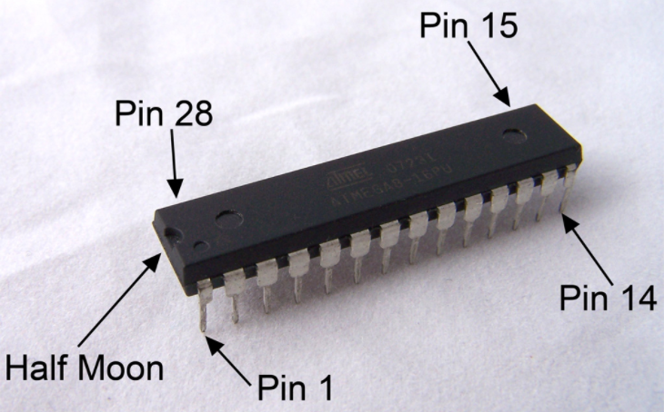
Each integrated chip has a marking that indicates the starting position of pin 1. Keeping the orientation of pin 1 and the direction of polarized components (capacitors, diodes, transistors, LEDs, etc.) consistent will facilitate PCB fabrication. Is this necessary?
If you’ve ever soldered or debugged a PCB yourself, you won’t doubt this. Just think about it: when the polarities and orientations of the components on the PCB are chaotic, don’t you feel uncertain about successfully soldering the PCB?
▲ Usually, there are small dots on the integrated chip package that indicate the position of pin 1. Keeping the orientation of all chips consistent will facilitate soldering and inspection.
Tip: Keep Component Positions Similar to the Schematic
When placing components, follow the positional relationships from your schematic in your mind. Why?
In fact, when you designed the schematic, you had already optimized the positional relationships between components (shortest connections, least crossings). Therefore, following the component positions from the schematic when placing PCB components has a natural rationale.
Especially during manual routing later, the schematic in your mind will subtly help you choose reasonable short paths for routing.
This article is reprinted from 巧学模电数电单片机, and the views in this article are neutral as per the Electronic Engineering Magazine, provided for learning and communication purposes.