Compared to single-sided and double-sided boards, the process flow of rigid multilayer printed circuit boards is fraught with challenges, with significantly increased difficulty, mainly reflected in the following aspects:
1.Inter-layer alignment of multilayer wiring
2.Alignment of holes with inner layer patterns
3.Step slot formation
4.Warping of the board surface
5.Defects such as internal delamination, bubbling, and voids
In response to the four industry-recognized technical pain points mentioned above, the following solutions are provided for reference:
1.Perform size pre-setting for each core board based on core material type, residual copper rate, and lamination parameters (collect size information for each product and establish a thermal expansion database for future use). Use PIN-LAM or MASS-LAM lamination positioning methods. According to the product stacking structure, stack and fix the core board, prepreg, and copper foil in sequence, then execute the first piece trial production. Test the inter-layer alignment accuracy of the first piece (x-ray or slicing), and adjust the core board pre-setting values based on the test results before proceeding to formal production.
2.After the lamination process, test the thermal expansion of the inner layer patterns, then scale the CNC drilling program accordingly and drill holes. The expansion test patterns should be symmetrically distributed relative to the center of the board and as far away from PIN pins or rivets as possible, while being close to the actual processed product. If the board surface is too large, it can be divided into sections, with a set of test patterns arranged in each section for sectional expansion drilling.
3.To reduce the component mounting surface, limit height, or reduce cascading height, the edges or interior of the printed board may have step slots of varying sizes and depths. Figure 1 shows two common types of step slots: one with metal on the bottom or side (left), and one with metal on both the bottom and side, forming a unified structure.
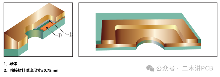
Figure 1 Two Typical Blind Slot Structures
The two most common methods for creating step slots are the filling spacer method and the reverse milling core board method, as shown in Figure 2.
Filling Spacer Method: Open a window in the prepreg adjacent to the bottom of the blind slot, and during stacking, fill the window position with a spacer of similar thickness. Before surface coating, use depth-controlled milling (depth control accuracy < prepreg thickness) to open the cover and remove the spacer. This method has a significant anti-adhesion effect, resulting in minimal overflow of resin at the bottom of the formed blind slot and high dimensional accuracy. However, filling and removing the spacer can be time-consuming, especially for small spacers that are prone to curling, with significant static adsorption phenomena, leading to a high risk of displacement.
Reverse Milling Core Board Method:Open a window in the prepreg adjacent to the bottom of the blind slot, and reverse mill the adjacent core board by about 2/3 of the board thickness, then proceed with stacking and lamination. Before surface coating, use depth-controlled milling (depth control accuracy < core board thickness) to open the cover and remove the spacer. This method is simple to operate, but the dimensional accuracy of the blind slot is relatively low, and the prepreg may overflow into the reverse milling tool path. Additionally, if the core board has low strength (such as in a PTFE resin system without glass fiber reinforcement), there may be protrusions in the area corresponding to the reverse milling path. Therefore, it is recommended to use a smaller diameter tool (D≤0.5mm) for reverse milling the core board (laser cutting can also be used, with the spot path generally less than 0.3mm).
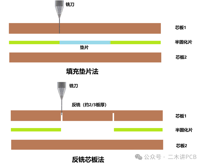
Figure 2 Methods for Forming Step Slots
4.Warping of the board surface can affect the assembly yield of components, especially for large pin count components such as FCBGA (Flipchip Ball Grid Array), LGA (Land Grid Array), and CCGA (Ceramic Column Grid Array). Due to environmental protection requirements, lead-free soldering is gradually replacing leaded soldering. Since the soldering temperature for lead-free soldering is generally more than 30°C higher than that for leaded soldering, lead-free soldering imposes higher requirements on the thermal resistance characteristics of materials. To reduce warping during high-temperature soldering, high Tg (Tg≥170°C) core boards should be selected. Additionally, warping of the board surface is caused by uneven stress at high temperatures, so the multilayer board stacking structure should be as symmetrical as possible, and copper should be laid in the blank areas without wiring. If the board contains materials such as PTFE, PPO, and FR4, which are mostly resin systems, and the stacking structure is asymmetrical, a thick metal core (such as copper, copper-indium-tin-copper, or copper-molybdenum-copper) can be inserted inside the board to reduce warping.
5.Defects such as delamination, bubbling, and voids within multilayer boards are mostly directly related to the lamination process.
a) Regularly test the parallelism and temperature uniformity of the hot plates in the press. If abnormalities are found, promptly contact the manufacturer for equipment maintenance.
b) Clean the lamination molds and the residual adhesive on the dividing steel plates at the end of each shift to prevent residual adhesive from falling and causing dents on the board surface.
c) Reasonably select spacer thickness, keeping the difference from the thickness of the opened prepreg within 30 microns, and regularly replace the pressure cushioning material.
d) Match the residual copper rate of the core board with the adhesive content of the prepreg to prevent insufficient filling of adhesive.
e) The surface color of the copper foil on the core board after browning or blackening should be uniform, and the micro-etching amount should meet the requirements.
The typical production process flow for rigid multilayer printed circuit boards is shown in Figure 3. The number of lamination cycles may vary depending on different stacking structures, and the process flow may also differ. Additionally, many factories have both acidic and alkaline etching processes, and there may be two electroplating steps after the drilling process.
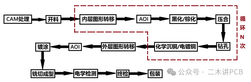 Figure 3 Typical Process Flow for Rigid Multilayer Printed Circuit Boards