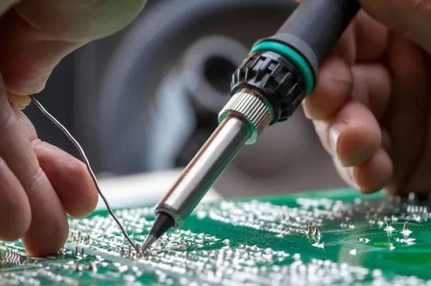
Reliability and Stability of PCB Soldering
With the accelerated iteration of smart terminal devices, PCBs, as the core carrier of electronic systems, have their soldering process reliability directly determining the product lifecycle. The modern electronic manufacturing field has formed a multi-dimensional quality assessment system. To ensure the reliability and stability of PCB soldering, strict inspection and analysis of soldering quality are required.

1. Types of Soldering Defects
Common soldering defects during the PCB soldering process include:
01. Solder Balls
Small spherical solder around component solder joints, which may cause short circuits between components.
02. Solder Cracking
Small cracks appearing inside the solder joint or at the connection with the pad, which may lead to joint failure under vibration or temperature changes.
03. Pad Lifting
Separation of the pad from the substrate, usually caused by thermal stress or poor soldering.
04. Solder Bridging
Solder connecting adjacent solder joints, which may cause short circuits.
05. Poor Soldering
Bubbles appearing inside the solder joint, affecting the electrical and mechanical performance of the joint.
2. Causes of Soldering Defects
01. Improper Temperature Control
Excessively high temperatures can lead to solder oxidation and the formation of solder balls, while too low temperatures may cause poor soldering and solder bridging issues.
02. Excessive Soldering Time
Prolonged soldering time can cause excessive flow of solder, leading to solder balls and solder cracking; too short a time may result in pad lifting, weakening the joint’s strength.
03. Mismatched Soldering Speed
Excessively fast soldering speed lacking precision may induce poor soldering and solder bridging, while too slow speed can cause uneven solder distribution, leading to solder balls or solder cracks.
04. Solder Quality
Using low-quality solder, which may contain impurities, can easily lead to solder cracking.
05. Improper Surface Treatment of the Substrate
If the surface treatment of the substrate is inadequate, it will make it difficult for the solder to wet evenly, potentially leading to poor soldering or solder cracking.
06. Design Issues
Soldering defects can sometimes be related to PCB design, such as unreasonable pad design or overly dense component arrangement, which may lead to poor soldering or solder bridging.
3. Soldering Quality Inspection Methods
01. Visual Inspection
First, visually inspect the appearance of the soldering area for issues such as cold solder, missed solder, uneven solder joints, and solder joint gloss. This is the most basic soldering quality inspection method and can quickly identify obvious defects.
02. X-ray Inspection
X-ray inspection is a non-invasive method that can penetrate PCB boards to detect defects in solder seams, including cold solder and irregular solder joint shapes. This method has high sensitivity for detecting soldering quality and can show the internal state of solder joints, such as voids and solder joint density.
03. Ultrasonic Inspection
Ultrasonic inspection can detect the surface and internal quality of the soldering area. Through high-frequency vibrations, ultrasound can probe solder joints to detect cracks, voids, and other issues. This method is suitable for detecting soldering defects and solder joint density.
04. Optical Inspection
Optical inspection covers two main areas: ultraviolet light detection with wavelengths from 700 to 1600 nanometers, and infrared light detection with wavelengths from 1000 to 1700 nanometers.
Ultraviolet light detection focuses on defects such as oxidation and residues on the surface of solder joints, while infrared light detection delves into the interior of solder joints to detect hidden issues like oxidation and voids.
05. Electrical Performance Testing
By performing electrical performance tests on the soldering area, such as resistance, capacitance, and inductance parameters, the soldering quality can be assessed. This method can directly test the performance of solder joints to determine if they meet design requirements.
06. Thermal Shock Testing
Thermal shock testing is an effective means to simulate solder joint performance under extreme temperature variations. By conducting thermal shock tests on the soldering area, the reliability and stability of solder joints can be evaluated, preventing issues under extreme temperatures.
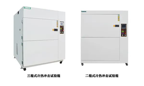
Wuhan Jin Ce Laboratory is equipped with two-box and three-box thermal shock test chambers, with a temperature testing range covering -55℃ to 150℃, and a basket conversion time of no more than 10 seconds, providing customized testing services based on customer needs.
Thermal shock testing is a key method to ensure that products maintain performance stability and reliability under extreme temperature fluctuations. By conducting rigorous thermal shock tests, the safety and lifespan of products can be enhanced, which is crucial for improving product quality and market competitiveness.
Wuhan Jin Ce Testing Technology Co., Ltd. has comprehensive capabilities for thermal shock testing of chips, electronic components, and PCBs, ensuring the accuracy and reliability of test data, and providing professional and convenient testing and analysis services for customers. For more details, please feel free to contact 027-81526660 or 18971200508, Mr. Cao.
Recommended Reading