
1. Purpose: To provide a basis for the appearance inspection of PCBA products produced at our SMT station. In cases where the specific appearance standards conflict with customer requirements, customer requirements shall prevail in principle.
2. Scope: This standard references IPC-610D (for dedicated service electronic products) PCBA appearance inspection standards and is applicable only to all PCBA products produced at our SMT station.
3. Definitions:
3.1 Standards:
3.1.1 Acceptance Criteria: The acceptance criteria include three conditions: ideal condition, acceptable condition, and nonconforming defect condition (rejection condition).
3.1.2 Ideal Condition: This assembly condition is close to the ideal and perfect assembly state. It is determined to be ideal if it has good assembly reliability.
3.1.3 Acceptable Condition: This assembly condition does not meet the ideal condition but can maintain assembly reliability, thus considered acceptable.
3.1.4 Nonconforming Defect Condition: This assembly condition fails to meet the standards and is determined to be a rejection condition.
3.1.5 Priority of Engineering Documents and Assembly Work Instructions: When the content of the appearance acceptance standards conflicts with engineering documents or assembly work instructions, the content of the other listed instructions shall take precedence; other special (customer) requirements not listed in the appearance acceptance standards may refer to the assembly work instructions or other guidelines.
3.2 Definition of Defects:
3.2.1 Critical Defect: Refers to defects that could cause harm to humans or machines, or endanger life and property safety, referred to as critical defects, denoted as CR.
3.2.2 Major Defect: Refers to defects that have lost practicality or caused a reduction in reliability of the product, resulting in damage or malfunction, referred to as major defects, denoted as MA.
3.2.3 Minor Defect: Refers to defects that do not materially reduce the usability of the unit and can still achieve the desired purpose, generally referring to differences in appearance or assembly, denoted as MI.
1. PCBA Semi-finished Product Handling Method
Ideal Condition:
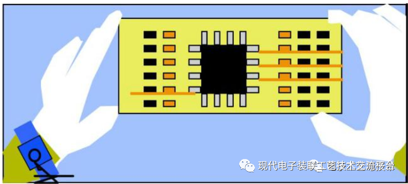
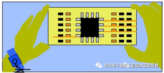
(a) Wear clean gloves and implement good electrostatic protection measures.
(b) Hold the board edges or corners for inspection.
Acceptable Condition:
(a) Wear good electrostatic protection measures, holding the PCB edges or corners for inspection.
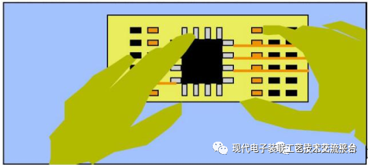
Nonconforming Defect:
Nonconforming Defect:
(a) No electrostatic protection measures are in place, and direct contact with conductors, gold fingers, and solder points occurs.
2. General Requirement Standards – 2.1 Solderability Terminology and Definitions:
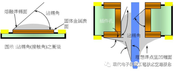
1. Wetting: The formation of solder adhesion on the surface, with a smaller wetting angle indicating better wetting.
2. Wetting Angle: The angle formed by the contact of the solid metal surface with the molten solder (as shown in the figure below), generally the angle at the interface between the liquid surface and the other soldered body or liquid; a smaller angle indicates better solderability.
3. Non-wetting: No solder adhesion is formed on the surface, with a wetting angle greater than 90 degrees.
4. De-wetting: The solder that was originally wetting retracts. Sometimes a very thin solder film remains, and as the solder retracts, the wetting angle increases.
5. Solderability: The surface characteristic that allows easy adhesion of molten solder.
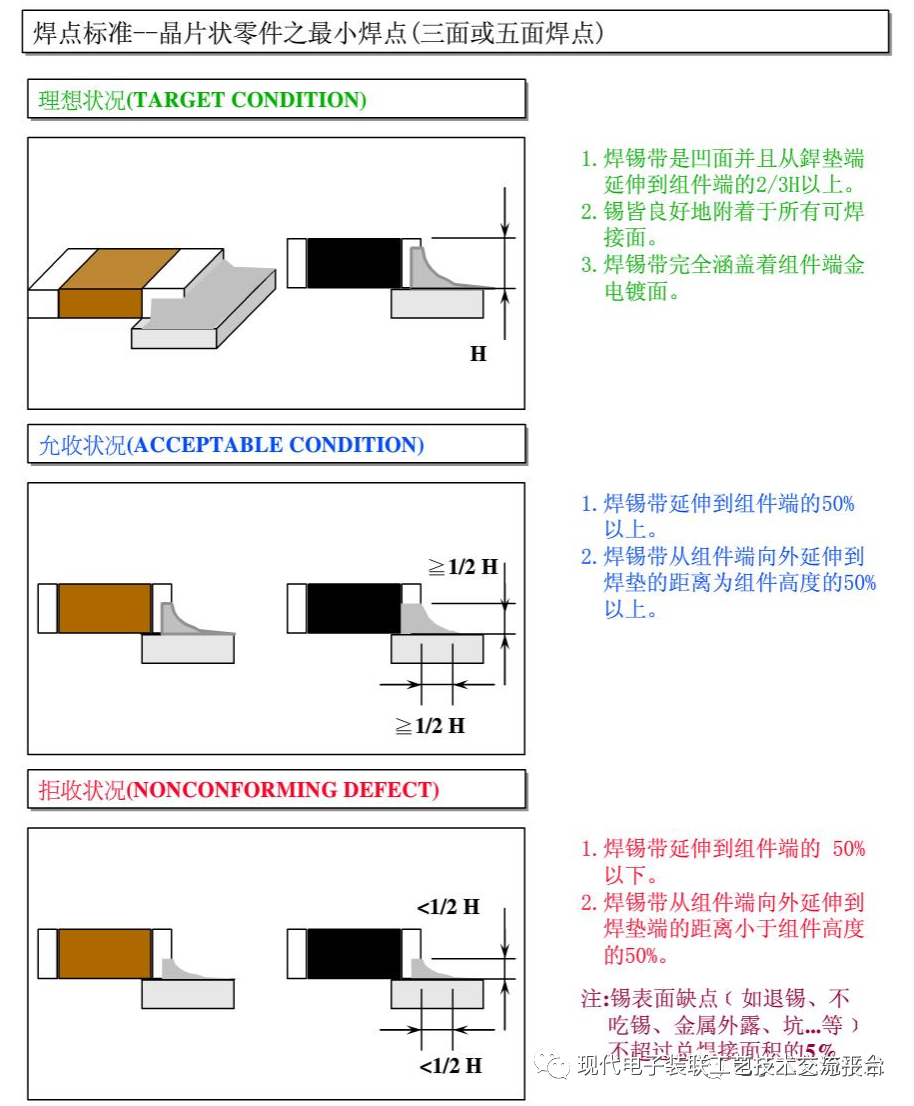
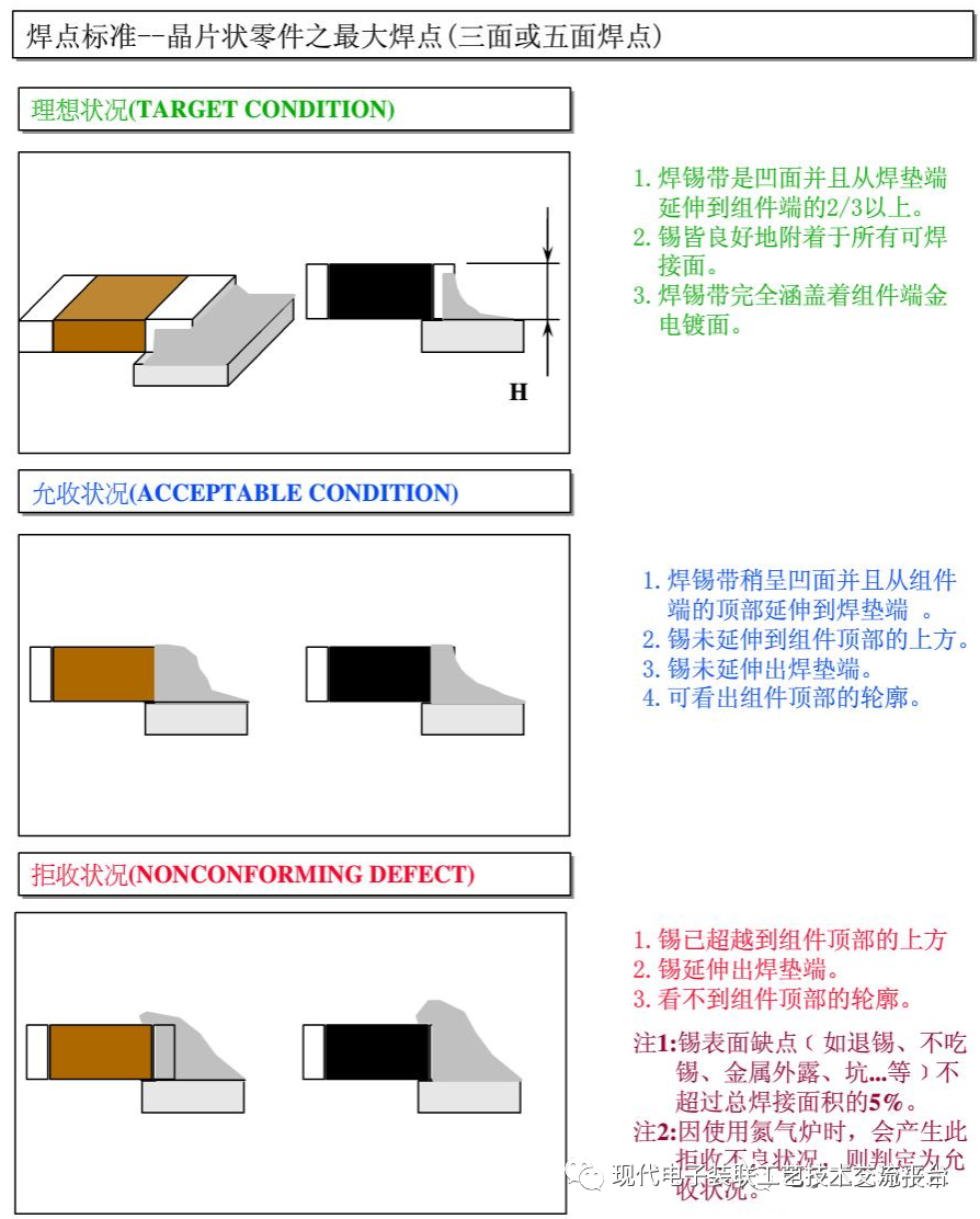
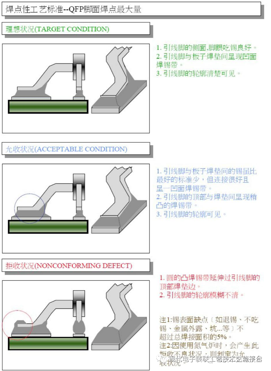
2.2 Ideal Solder Joint Process Standards:
Ideal Solder Joint Process Standards:
1. The solder joints appearing on the solder side should be solid, flat-topped, and conical; the outer edges should present a crescent-shaped uniform arc, and the solder in the through-hole should completely and uniformly cover the component leads.
2. The bottom area of the conical solder joint should match the pad on the board (LAND, PAD, ANNULAR RING) such that over 95% of the solder surface extends into the pad.
3. The amount of solder should be appropriate to fill the edges of the pad and component leads, and the wetting angle should approach zero; the smaller the wetting angle, the better the solderability.
4. The solder surface should be shiny (unless affected by other factors, such as contamination by chemicals that cause loss of luster); the surface should be smooth, uniform, and free of irregularities such as small notches, bubbles, inclusions, or protrusions.
5. For solder in plated through-holes, the solder should flow into the hole and rise to the component side, and the solder on the solder side should be smooth, uniform, and meet the criteria described in point 4.
In summary, good solderability should have a shiny solder surface and a wetting angle close to zero. The soldering condition is determined as follows based on the wetting angle:
0 degrees < 0 < 90 degrees acceptable soldering: ACCEPTABLE WETTING
90 degrees < 0 unacceptable soldering: REJECT WETTING
2.3 General Requirement Standards – Solderability Process Level:
2.3.1 Solder Cracking:
1. No solder joint cracking is allowed.
2.3.2 Solder Spikes:
1. No solder spikes are allowed; visible solder spikes must be trimmed, and solder spikes are deemed unacceptable.
2. Solder spikes (after trimming) must meet the standard length of component leads (2.0mm).
2.3.3 Solder Holes/Pinhole:
1. Solder holes/pinholes visible under three times magnification are not accepted. 2. Solder holes/pinholes must not penetrate through the hole.
3. No de-wetting or non-wetting defects are allowed.
2.3.4 Breakthrough Holes/Burst Holes:
1. No breakthrough or burst holes are allowed.
2.3.5 Solder Bridges (Short Circuits):
1. No solder bridges are allowed that create short circuits between two conductors.
2.3.6 Solder Dross:
1. Solder dross visible under three times magnification is not accepted.
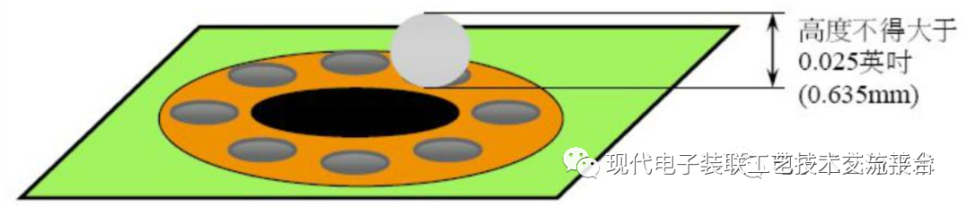
2.3.7 Excessive Solder in Assembly Screw Holes:
1. The height of solder beads and spikes on the solder pads of assembly screw holes on the component side must not exceed 0.025 inches.
2. Excessive solder must not appear on the solder surface of assembly screw holes.
3. The inner walls of assembly screw holes must not be soldered.
2.4 General Requirement Standards – PCB/Component Requirement Standards:
2.4.1 PCB/Component Damage – Minor Damage:
1. Minor damage is acceptable.
Scratches and scuff marks on the body of plastic or ceramic components are acceptable as long as the internal components are not exposed. Minor scratches on the component body are acceptable as long as they do not damage the component packaging or cause unclear component markings.
2. PCB Delamination/Bubbling:
1. No PCB delamination (DELAMINATION) or bubbling (BLISTER) is allowed.
2.4.2 PCB Cleanliness:
1. No foreign impurities such as cut component leads, (obvious) fingerprints, or dirt (dust) are allowed.
2. If the materials of the components, such as thermal pads and adhesive, are misaligned, they will not be accepted.
3. Residues of no-clean flux (such as watermarks) are acceptable; a thin layer of white residue (such as watermarks) is acceptable, but powdery, granular, or crystalline residues are not acceptable.
4. Compliance with solder bead and solder dross standards (including visible rejection).
5. Loose metal burrs on component leads are not acceptable.
2.4.3 Gold Finger Requirement Standards:
1. Gold fingers must not be lifted or damaged; contact areas may be damaged but must not be lifted.
2. Important areas of gold fingers must not have any form of solder, including any size of solder balls, solder dross, or stains.
3. Other minor defects in the contact area of gold fingers exceeding 0.010 (0.25mm) inches are not accepted.
2.4.4 Scratches:
1. Scratches that reach the PCB fiber layer are not accepted.
2. Scratches that expose copper traces on the PCB are not accepted.
2.4.5 Appendix Unit Conversion:
1 mil (mil) = 0.001 inches (inch) = 0.0254 millimeters (mm) 1 inch = 1000 mils (mil) = 25.4 millimeters (mm)
2.5 General Requirement Standards – Other Requirement Standards:
2.5.1 Polarity:
1. Polarized components must be placed according to the work instructions or PCB markings, ensuring correct polarity.
2.5.2 Component Marking Printing:
Marking printing, identification, or other identification codes must be legible, except in cases where the component supplier has not marked them.
2.5.3 Heat Sink Bonding (Thermal Paste Application):
1. Central Processing Unit (CPU) thermal paste application:
The assembly standards for heat sink bonding (heat sink connection) must comply with the work instructions:
2. Non-Central Processing Unit (CPU) thermal paste application:
Heat sink bonding (thermal paste application) must comply with the work instructions.
Excessive thermal paste application and fingerprints on the board surface are not acceptable.
This account is non-profit, and this article is sourced from online articles for sharing and educational purposes only. The text, images, etc. in this article are reprinted from the internet, and the copyright belongs to the original author. If the relevant rights holder has any objections, please contact us as soon as possible, and we will delete it promptly. The content of this article represents the views of the original author and does not represent the views of this public account or its responsibility for its authenticity.

Electronic Assembly Process Technology WeChat Group (Note: Company + Name)

Electronic Assembly Process Technology QQ Group (Note: Company + Name)
Long press to recognize the QR code to follow the [Modern Electronic Assembly Process Technology] subscription account and start our shared learning journey.

Recommended Reading:
SMT Appearance Inspection Standards PPT – Very Good!!!
Reflow Soldering Process – Collector’s Edition PPT
SMT Reflow Oven Temperature Curve Analysis – Collector’s Edition PPT
SMT Soldering Defects and Inspection Techniques (Worth Collecting)
The Eight Wastes of Lean Production – PPT
Three-proofing and Sealing, and Mixed PCB Rework Technology
Three-proofing Process Technology for Printed Circuit Board Assemblies (Useful Content)
Electronic Wiring Harness Process Flow Lecture
Manual Soldering Process Technology Training Materials
Training Information:
Cleaning, Coating, and Three-proofing Process Technology and Case Analysis for Electronic Products July 17-18, 2020 Beijing
Practical Multi-core Cable Assembly Technology and Fault Analysis June 18-19, 2020 Beijing
Reflow Soldering Technology and Misconceptions Analysis June 18-19, 2020 Beijing
New Military Product Equipment Identification and Review June 16-17, 2020 Shanghai
SMT New Technology Lecture on Special Process Application Technology July 16-17, 2020 Shanghai
Advanced Seminar on Modern Electronic Assembly Process Technology and Engineering Quality Defect Analysis July 14-15, 2020 Beijing
Recommended Books:
Surface Mount Technology (SMT) Basic Process Book Recommendations