Yesterday, we published the article “Call for Papers on PCBA Design and Manufacturing,” and we welcome everyone to submit their contributions.
1. Why Do PCBs Need Surface Treatment?
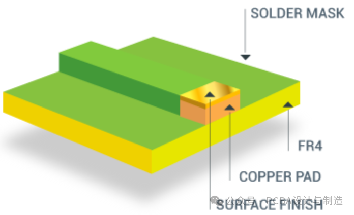
The core purpose of PCB surface treatment is to: protect copper pads and ensure their solderability..
1. Prevent pad oxidation: Copper easily oxidizes in air, and the resulting copper oxide severely weakens solderability, leading to cold solder joints.
2. Provide a solderable layer: To provide a uniform, reliable, and easy-to-solder metal layer for subsequent component soldering.
3. Meet electrical performance requirements: Certain treatments (such as ENIG) can provide a stable contact interface for gold fingers, buttons, etc.
4. Adapt to complex assembly processes: For example, wire bonding requires a pure gold surface, while crimp connections require a hard gold surface.
2. What Standards Exist for PCB Surface Treatment?
1. IPC-455X series special standards
① IPC-4552B: Specification for Electroless Nickel/Immersion Gold (ENIG)
② IPC-4553A: Immersion Silver Specification
③ IPC-4554: Immersion Tin Specification
④ IPC-4555: High-Temperature Organic Solderability Preservative (OSP) Specification
⑤ IPC-4556: Electroless Nickel/Palladium/Immersion Gold (ENEPIG) Specification
⑥ IPC-2221C: Generic Standard for Printed Board Design
2. National Standards
① SJ 20818-2002: Metal Coating and Chemical Treatment for Electronic Equipment
② GB 51291-2018: Design Standards for Co-fired Ceramic Hybrid Circuit Substrates
3. Detailed Explanation of PCB Surface Treatment Processes
Common PCB surface treatment processes include Hot Air Solder Leveling (HASL), Organic Solderability Preservative (OSP), Electroless Tin (I-Sn), Electroless Silver (I-Ag), Electroless Nickel/Gold (ENIG), Electroless Nickel/Palladium/Gold (ENEPIG), and Selective Electroless Nickel/Gold (ENIG+OSP).
1. Hot Air Solder Leveling (HASL)
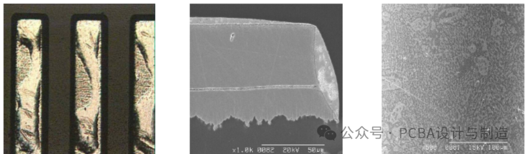
① Definition
This process involves immersing the printed circuit board in molten solder and then using hot air to blow away excess solder from the surface and metallized holes, resulting in a smooth, uniform, and appropriately thick solder coating. This process utilizes the wetting action of molten solder to achieve bonding between copper traces and solder.
② Process Flow
The cleaned printed circuit board is immersed in molten solder for a certain period, then removed and excess solder is blown away using a hot air knife, ensuring uniform solder coating thickness. The general process flow for hot air leveling includes: micro-etching – preheating – applying flux – soldering – cleaning.
③ Typical Thickness
1~40μm.
④ Advantages
HASL technology is mature, cost-effective, can achieve double-sided processing, suitable for thick copper, has good flatness, and is reworkable.
⑤ Disadvantages
Poor surface flatness; lead-containing processes do not comply with RoHS regulations; unsuitable for fine-pitch components; potential for solder beads; high surface treatment temperature may affect substrate and solder mask performance; due to the relatively thick coating, compensation for drill hole diameter is necessary.
⑥ Failure Modes
Poor flatness of the solder layer after hot air leveling can lead to cold solder joints during soldering; oxidation or corrosion of the solder layer after long-term use can reduce soldering performance; under thermal stress, fatigue cracks may occur at the interface between the solder layer and copper substrate, reducing soldering reliability.
⑦ Theoretical Basis
Utilizing the wetting principle of solder on copper, molten solder spreads on the copper surface to form a solder layer, and hot air removes excess solder to ensure uniform thickness. The involved physicochemical processes include solder wetting, spreading, and the formation of intermetallic compounds (IMC) between copper and solder (such as Cu₆Sn₅, Cu₃Sn), which significantly affect soldering strength and reliability, while also considering factors like solder surface tension on coating flatness.
2. Electroless Nickel/Gold (ENIG)
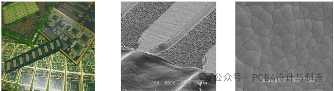
① Definition
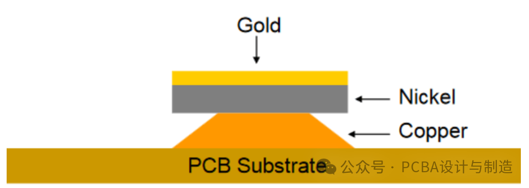
This process involves depositing a layer of nickel-phosphorus alloy on the copper surface of the printed circuit board through a chemical method, followed by depositing a layer of gold. The nickel layer acts as a barrier to prevent copper from reacting with subsequent solder or gold, while the gold layer provides good solderability and oxidation resistance.
② Process Flow
After cleaning and micro-etching the PCB surface, the processes of electroless nickel and electroless gold are performed sequentially. Electroless nickel is deposited under catalytic conditions, where nickel ions are reduced and deposited on the copper surface; electroless gold is then deposited on the nickel layer. The general process flow for electroless nickel-gold includes: acidic cleaning – micro-etching – pre-soaking – activation – electroless nickel – electroless gold.
③ Typical Thickness
Nickel layer: 3~5μm; Gold layer: 0.05 – 0.25μm.
④ Advantages
Flat pads, uniform thickness, good solderability and oxidation resistance, widely used, suitable for fine pitch, and a smooth surface beneficial for subsequent soldering and testing.
⑤ Disadvantages
High cost, nickel layer prone to “black pad” phenomenon, solderability greatly affected by process parameters, nickel layer is brittle, and the process is complex.
⑥ Failure Modes
Improper chemical processes can lead to “black pad” in the nickel layer, resulting in poor solderability; uneven gold layer thickness or high porosity can lead to nickel oxidation (from pores), affecting soldering; poor adhesion between the nickel-phosphorus alloy layer and copper substrate can cause delamination and other defects.
⑦ Theoretical Basis
Based on the principles of redox reactions in electroless plating, nickel deposition occurs when nickel ions are reduced by reducing agents such as sodium hypophosphite, and gold deposition occurs when gold ions are reduced. The nickel layer acts as a barrier to prevent copper from forming harmful intermetallic compounds with solder or gold, while the gold layer provides low contact resistance and good solderability, involving electrochemical principles such as electrode potential, reaction kinetics, and the formation and control of intermetallic compounds.
3. Electroplated Nickel/Gold
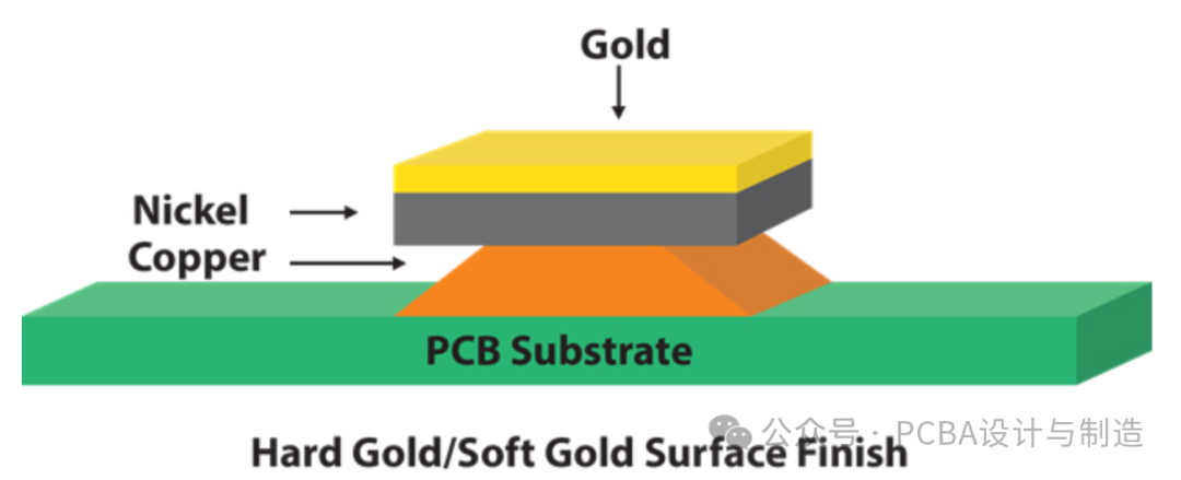
① Definition
This process uses electroplating principles to first plate nickel on the copper surface of the printed circuit board, followed by gold plating. Nickel and gold ions are deposited on the copper surface through the application of external current.
② Process Flow
After pre-treatment, the PCB undergoes electroplating of nickel and gold in the electroplating tank, controlling current, time, and other parameters to achieve the desired layer thickness.
③ Typical Thickness
Nickel layer: typically 25~50μm; Gold layer: 0.05~0.5μm.
④ Advantages
Good flatness, accurate layer thickness control, suitable for high reliability requirements, can perform thick gold plating (such as gold fingers), and has a long service life.
⑤ Disadvantages
High cost, nickel layer prone to internal stress, significant equipment investment, and complex process control.
⑥ Failure Modes
Impurities in the electroplating solution can lead to poor nickel layer crystallization and poor solderability; after wear, the gold layer can oxidize the nickel layer, affecting contact performance; high internal stress in the coating can lead to cracking.
⑦ Theoretical Basis
Based on the principles of electroplating, under the influence of an external direct current field, nickel and gold ions are reduced and deposited on the cathode (copper surface). The role of the nickel layer is similar to that of electroless nickel, acting as a barrier, while the gold layer provides solderability and corrosion resistance, involving theoretical aspects such as electrode process kinetics, dispersion ability, and covering ability of the electroplating solution.
4. Gold Plating (Hard Gold, Soft Gold)
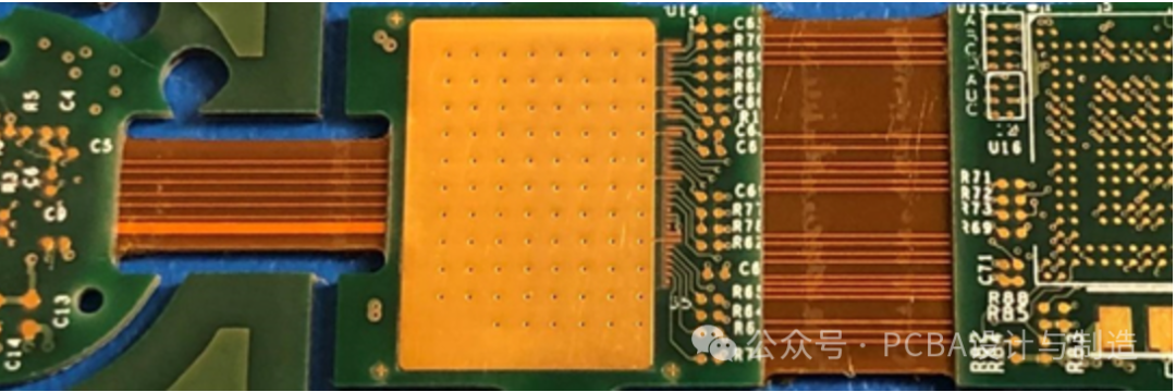
① Definition
This process involves electroplating a layer of gold on the surface of the printed circuit board, classified into hard gold (with added elements like cobalt) and soft gold (pure gold or with a small amount of other elements), primarily used to provide good solderability and electrical contact performance.
② Process Flow
After pre-treatment, gold plating is performed in the electroplating tank, controlling current, temperature, and electroplating solution composition to achieve the desired hardness and thickness of the gold layer.
③ Typical Thickness
0.5μm.
④ Advantages
Good flatness, low contact resistance, wear resistance (hard gold), and a long service life.
⑤ Disadvantages
High cost.
⑥ Failure Modes
Wear, stress cracking, corrosion.
⑦ Theoretical Basis
Utilizing electroplating principles, gold ions are reduced and deposited on the cathode (PCB surface). The alloying elements added to hard gold alter the crystal structure of gold, increasing hardness, suitable for high-wear electrical contact areas; soft gold has good solderability, involving basic theories of electroplating such as Faraday’s law and electrode reactions.
5. Organic Solderability Preservative (OSP)
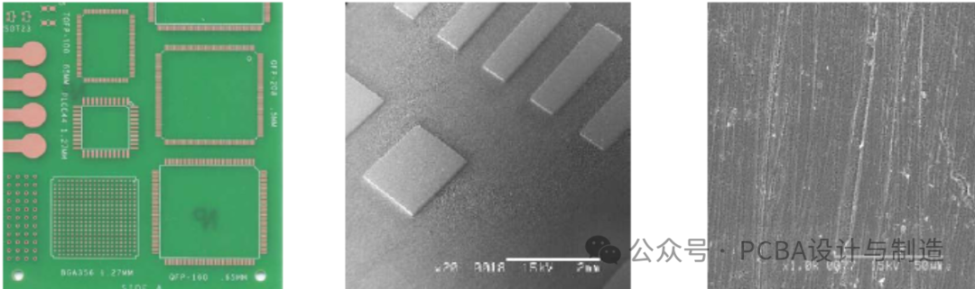
① Definition
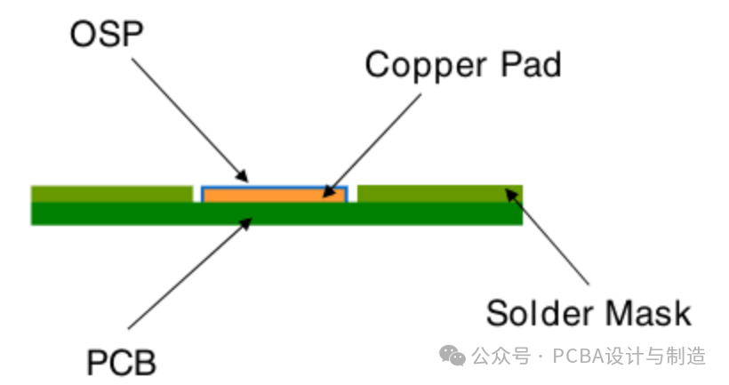
“Organic Solderability Preservative (OSP)” is a layer of organic compound film that covers the clean bare copper surface, which has properties of oxidation resistance, heat resistance, and moisture resistance, and can be dissolved by molten solder during soldering, allowing direct contact between bare copper and solder, thus facilitating the soldering reaction.
② Process Flow
De-oiling, micro-etching, acid cleaning, pre-soaking, OSP coating, curing (optional)
③ Typical Thickness
Approximately 0.5μm.
④ Advantages
Environmentally friendly, suitable for fine lines, low cost, simple process, can be reflow soldered multiple times, smooth surface, and high production efficiency.
⑤ Disadvantages
Short usage cycle, cannot be stored for long periods, surface is easily mechanically damaged, film thickness on PTH holes may be uneven, and soldering requires precise control of process parameters; otherwise, issues like cold solder joints and bridging may occur, requiring high cleanliness for subsequent assembly.
⑥ Failure Modes
Poor process control (e.g., insufficient chemical treatment) leads to poor protective effect of the film, copper oxidation; film is scratched or contaminated, losing protective function; uneven dissolution of the film during soldering leads to poor soldering.
⑦ Theoretical Basis
Based on the principle of organic compounds adsorbing on the copper surface, the protective film forms through physical and chemical adsorption, preventing copper oxidation. During soldering, high temperatures cause the organic film to dissolve, allowing copper to directly contact solder, facilitating wetting and spreading, involving theories of adsorption in surface chemistry and wetting during soldering.
6. Electroless Silver (I-Ag)
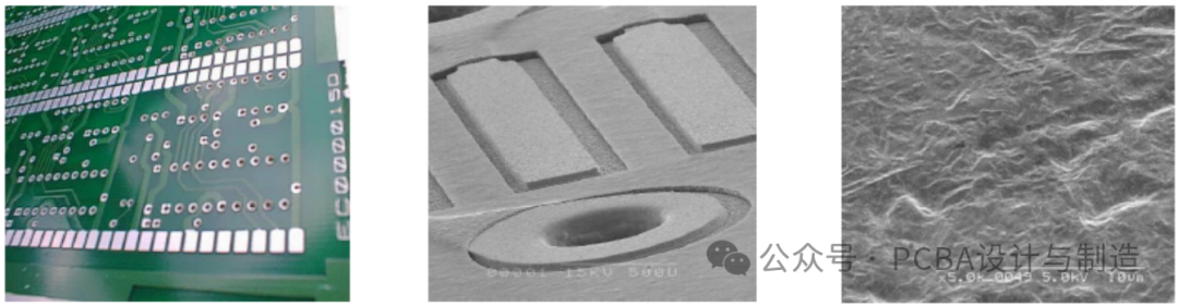
① Definition
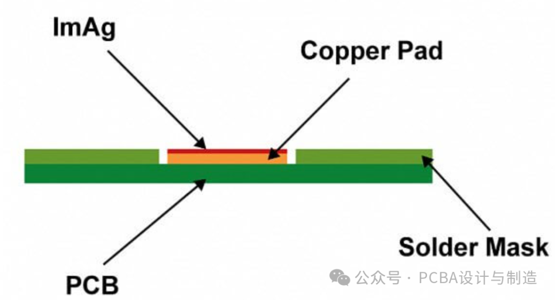
“Electroless Silver” is a process that deposits a layer of silver on a clean bare copper surface through a chemical displacement reaction, providing good solderability and oxidation resistance, while also preventing copper from reacting with solder to some extent.
② Process Flow
De-oiling, micro-etching, acid cleaning, pre-soaking, electroless silver, post-treatment (optional)
③ Typical Thickness
0.1~0.4 μm.
④ Advantages
Environmentally friendly, suitable for fine lines, low cost, simple process, can be reflow soldered multiple times, smooth surface, high production efficiency, and provides good solderability and conductivity.
⑤ Disadvantages
Silver is prone to sulfide formation, requiring special storage and usage conditions; high control requirements for silver layer thickness, otherwise silver ion migration may occur, leading to circuit short circuits.
⑥ Failure Modes
Poor surface treatment of the silver layer leads to sulfide formation, affecting solderability; silver ion migration causes circuit failures; improper control of the silver deposition process leads to poor adhesion of the silver layer to the copper substrate, resulting in delamination.
⑦ Theoretical Basis
Utilizing chemical displacement reactions, copper acts as a reducing agent to reduce silver ions to silver atoms deposited on its surface (Cu + 2Ag⁺ = Cu²⁺ + 2Ag). The solderability of the silver layer is due to its good wetting properties, and its oxidation resistance is because silver is relatively stable in air, but sulfide formation is a chemical process that needs attention, involving the kinetics of redox reactions and the corrosion and protection theories of metals.
7. Electroless Tin (I-Sn)
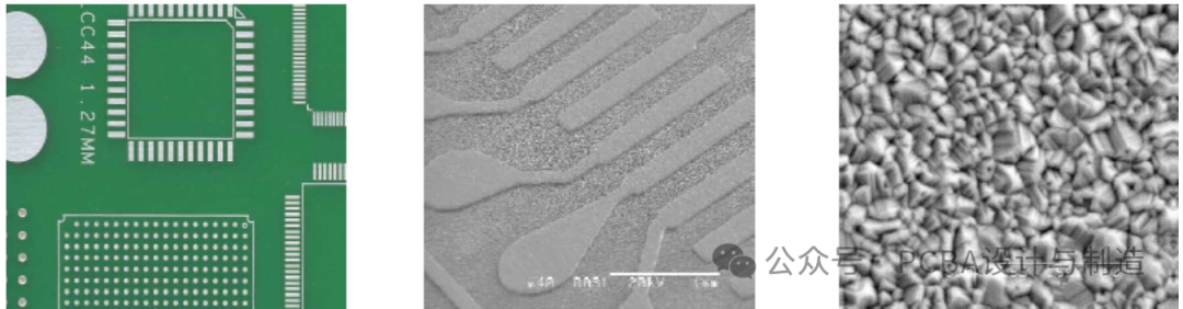
① Definition
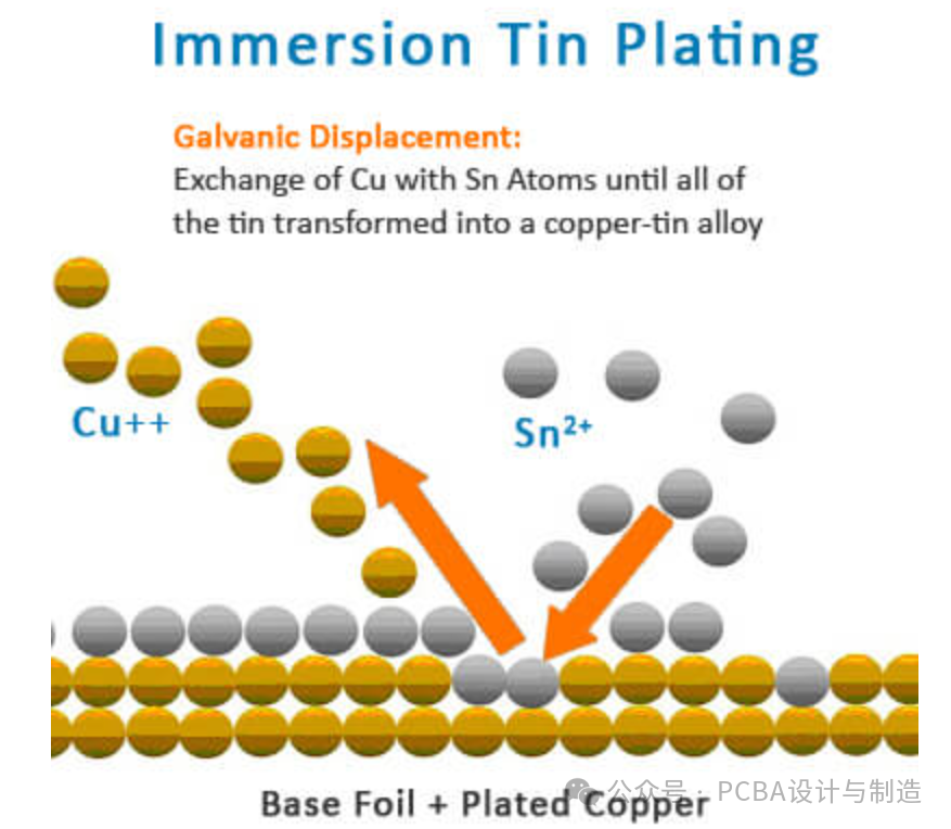
“Electroless Tin” is a process that deposits a layer of tin on a clean bare copper surface through a chemical displacement reaction, providing good solderability and preventing copper oxidation.
② Process Flow
De-oiling, micro-etching, acid cleaning, pre-soaking, electroless tin, post-treatment.
③ Typical Thickness
0.1~1.2μm.
④ Advantages
Environmentally friendly, suitable for fine lines, low cost, simple process, can be reflow soldered multiple times, smooth surface, high production efficiency, and good compatibility with solder.
⑤ Disadvantages
Tin is relatively soft, easily scratched or can produce “tin whiskers,” which may cause circuit short circuits; deposition processes need to be controlled to reduce tin whisker formation, and storage conditions are critical.
⑥ Failure Modes
Tin whiskers on the surface can cause circuit short circuits; oxidation of the tin layer (in harsh environments) affects solderability; improper control of the tin deposition process can lead to poor adhesion of the tin layer to the copper substrate, resulting in peeling.
⑦ Theoretical Basis
Based on chemical displacement reactions, copper reduces tin ions to tin deposited on the surface (Cu + Sn²⁺ = Cu²⁺ + Sn). The solderability of tin is due to its ability to dissolve with tin in the solder, forming a good soldering interface, involving redox reactions and theories of metal solderability, while the growth of tin whiskers relates to the crystal structure and internal stress of tin, falling under the category of crystal defects and diffusion theory in metallurgy.
8. Electroless Nickel/Palladium/Gold (ENEPIG)
① Definition
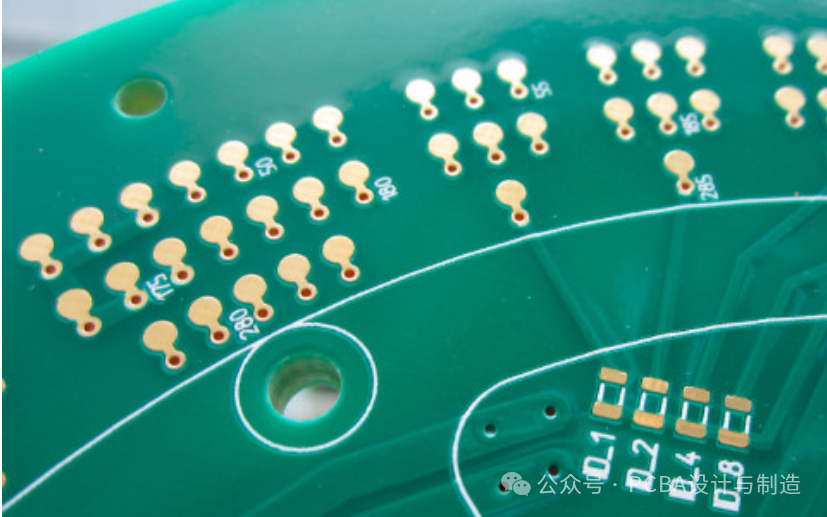
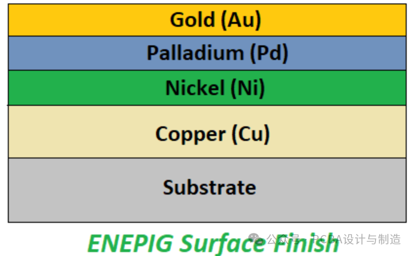
Electroless Nickel/Palladium/Gold (ENEPIG) is a newer surface treatment technology that adds a layer of palladium between nickel and gold compared to ENIG, further protecting the nickel layer from corrosion and preventing the “black pad” phenomenon that may occur with ENIG, thus offering better surface smoothness.
② Process Flow
Pre-treatment – De-oiling – Micro-etching – Acid cleaning – Pre-soaking and activation – Electroless Nickel (EN) – Electroless Palladium (EP) – Electroless Gold (IG) – Post-treatment.
③ Typical Thickness
Nickel deposition thickness is approximately 2~5μm.
Palladium thickness is approximately 0.05~0.20μm.
Gold thickness is 0.02~0.1μm.
④ AdvantagesExtremely flat surface, suitable for wire bonding, can be reflow soldered multiple times, high reliability of solder joints, and long shelf life.⑤ DisadvantagesExpensive, gold wire bonding is not as reliable as soft gold, prone to solder beads, complex process, and difficult to control during processing.
⑥ Failure Modes
Poor adhesion of the coating: If pre-treatment (de-oiling, micro-etching, activation) is insufficient, it may lead to poor adhesion of the nickel layer to the substrate, causing bubbling or peeling of the coating.
Palladium layer quality issues: If the palladium layer has pores, missing plating, or uneven thickness, it may not effectively block nickel diffusion, posing potential risks in specific environments (though the probability is very low).
“Gold embrittlement” phenomenon: If the gold layer is too thick, excessive gold entering the solder during welding can form brittle intermetallic compounds (IMC) such as AuSn₄. This IMC is brittle and can reduce the mechanical strength of the solder joint, making it prone to cracking under thermal or mechanical stress. Therefore, strict control of gold layer thickness is crucial.
Poor solder joints/wetting issues: If the coating surface is contaminated, oxidized, or the palladium layer is not fully covered by gold, it may lead to poor wetting during soldering, resulting in cold solder joints.
⑦ Theoretical Basis
The electroless nickel-palladium-gold process utilizes the electrochemical properties of metals, where precious metal ions in solution are dissolved at the anode and deposited as an alloy film on the workpiece surface through applied voltage. The principles mainly include anode dissolution, cathodic gold deposition, and substrate deposition processes. Nickel, palladium, and gold have a certain affinity, and by adjusting the composition of the electrolyte and process parameters, layered deposition of nickel, palladium, and gold can be achieved to form an alloy film.