To properly place SMT components, the PCB must remain completely flat. For accurate placement, the pick-and-place machine must release the SMT components at the same height above the circuit board for all components.
If the PCB is warped, meaning it is not flat, the machine cannot maintain a constant height when placing components on the board, which affects placement accuracy, especially for fine-pitch components.
Additionally, a flat PCB helps keep SMT components in the correct position during reflow. If high temperatures in the reflow oven cause changes in the flatness of the PCB, SMT components may float on molten solder and slide out of position, leading to solder bridging and opens.
1. What is PCB Warpage?
PCBs are typically made from fiberglass and other composite materials, and most PCBs are laminated only once and are very simple.
PCB warpage is the deformation of the PCB shape, as shown in the figure below, which clearly illustrates PCB warpage.
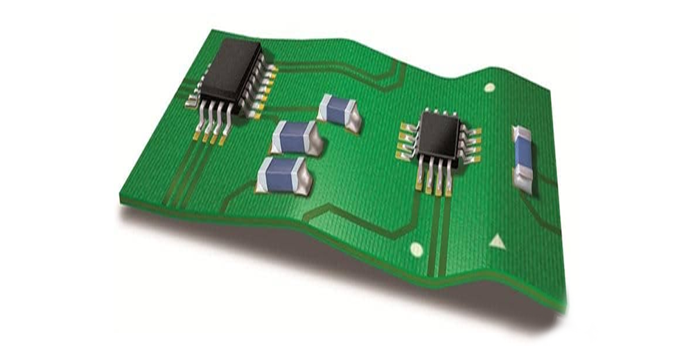
PCB Warpage
2. What is the Standard for PCB Warpage?
According to the IPS standard, the required warpage degree (WD) for the mounted PCB should be less than or equal to 0.75%. This means that when WD is greater than 0.75%, it should be judged as warped or a defective product.
In practice, when there are no components installed, and only through-hole components are needed, the flatness requirement is lower, and the WD standard can be less than or equal to 1.5%.
Of course, some manufacturers, to meet higher customer demands, may pursue stricter standards, with some WD standards needing to be less than or equal to 0.5%, or even less than or equal to 0.3%.
3. How to Calculate PCB Warpage?
Warpage, as the name suggests, refers to whether the PCB is flat and whether it can fit perfectly into the holes and surface mount pads of the board.
Warpage typically refers to the deformation where the surface of the plastic part does not conform to the designed shape. There are many factors that affect warpage, so it is essential to pay attention during the production process. After all, every small error could render the entire PCB scrap. So, how is PCB warpage calculated?
The formula for calculating PCB warpage is:
Warpage = Single Angle Warpage Height / (Diagonal Length of PCB * 2) * 100%
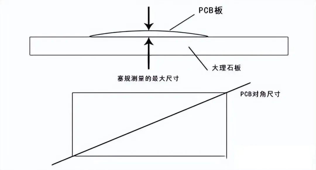
PCB Warpage Calculation Formula
In automatic insertion, if the PCB is not flat, it can cause inaccurate positioning, and may even lead to the automatic insertion machine freezing. If the board bends after component soldering, it becomes very difficult to trim the component leads neatly, ultimately leading to the PCB being unable to fit into the sockets in the chassis or machine, effectively scrapping the circuit board. For manufacturers, encountering PCB warpage is a painful issue.
4. Causes of PCB Warpage
1. Causes of PCB Warpage
1) The weight of the circuit board itself can cause the board to sag and deform.
Generally, the reflow oven uses a chain to drive the circuit board to move forward within the reflow oven, supporting the entire board at the two sides as the pivot points.
If there are heavy objects on the board, or if the board is oversized, due to the weight of the board, depressions may occur in the middle, leading to warpage.
2) Excessively deep V-cuts can cause warpage at the V-cut areas on both sides.
Essentially, V-Cuts are the main culprits that compromise the board’s structure since V-Cuts create grooves in the original large material, making them prone to warpage.
The materials, structure, and patterns all affect board warpage: PCBs are pressed from core boards, prepregs, and outer copper foils. The core board and copper foil can deform due to heat when pressed together. The amount of warpage depends on the coefficients of thermal expansion (CTE) of the two materials.
The CTE of copper foil is approximately 17X10-6; while the Z-direction CTE of ordinary FR-4 substrate below the Tg point is (5070)X10-6; above the Tg point it is (250350)X10-6. Due to the presence of glass cloth, the X-direction CTE is generally similar to that of copper foil.
2. Warpage Caused During PCB Processing
The causes of PCB processing warpage are complex and can be divided into thermal stress and mechanical stress.
Thermal stress mainly occurs during the pressing process, while mechanical stress mainly occurs during stacking, handling, and baking of the boards.
1) Warpage caused during the copper-clad board process
Copper-clad boards are all double-sided, with a symmetrical structure and no patterns. The CTE of copper foil and glass cloth is almost the same, so there is hardly any warpage caused by different CTE during the pressing process.
However, the copper-clad press is relatively large, and temperature differences in different areas of the heating plates can lead to slight differences in the curing speed and degree of resin in different areas during the pressing process. At the same time, the dynamic viscosity at different heating rates can also vary significantly, which can cause local stress due to the differences in the curing process.
Generally, this stress will remain balanced after pressing, but will gradually release and deform during subsequent processing.
2) Warpage caused during PCB pressing
The PCB pressing process is the primary process that produces thermal stress. Similar to the pressing of copper-clad boards, local stress can also occur due to different curing processes. Due to the thicker thickness, diverse pattern distribution, and more prepreg, thermal stress is more challenging to eliminate than with copper-clad boards.
The stress in the PCB will release during subsequent drilling, forming, or baking processes, leading to board deformation.
3) Warpage caused during solder mask and silkscreen baking
During the curing process, solder mask inks cannot stack on top of each other, and the PCB will be placed in a rack for baking to cure the board.
The solder mask temperature is around 150°C, exceeding the Tg value of the copper-clad board, making the PCB more prone to softening and unable to withstand high temperatures. Manufacturers must evenly heat both sides of the substrate while keeping the processing time as short as possible to reduce warpage.
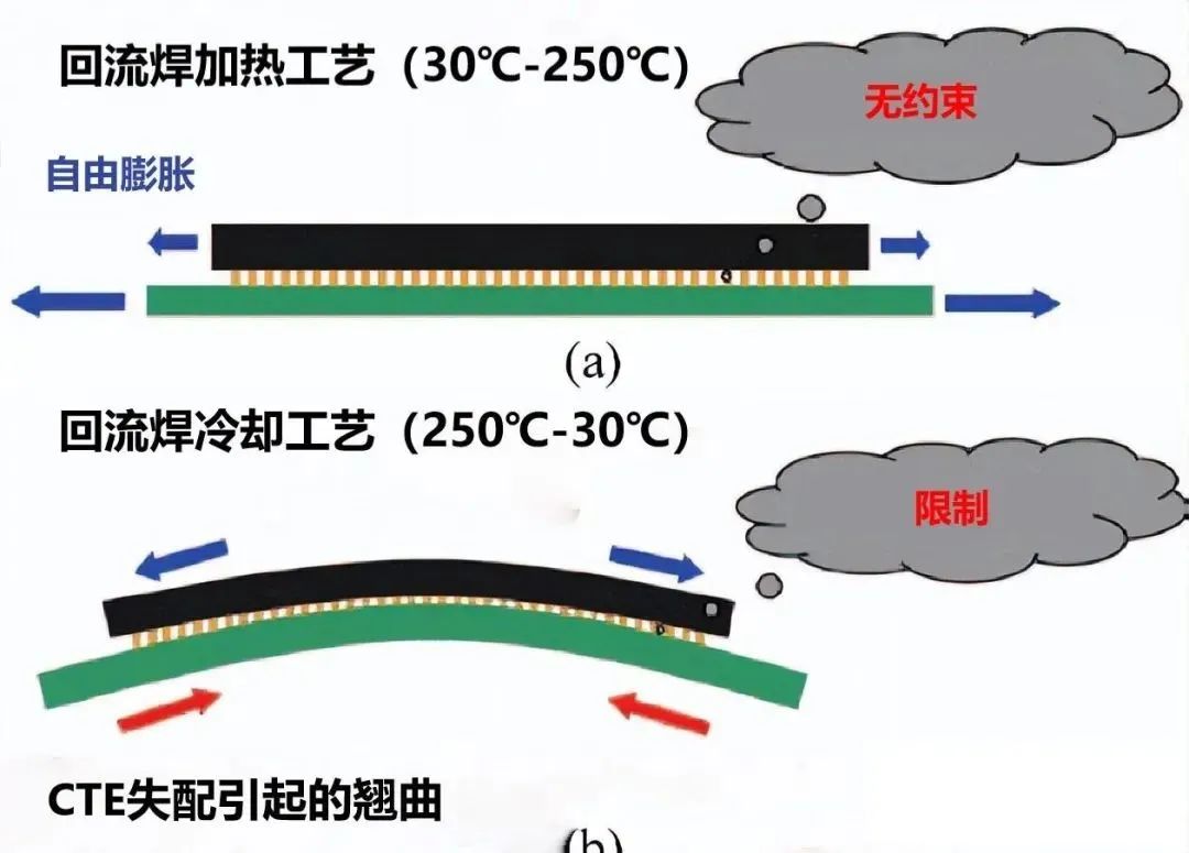
PCB Warpage
4) Warpage caused during cooling and heating processes
The temperature of the solder pot is between 225°C and 265°C, and the normal board hot air solder leveling time is 3s to 6s. The hot air temperature is between 280°C and 300°C.
After solder leveling, the board is placed in the solder pot from room temperature, and washed in room temperature water within two minutes after being removed from the pot. The entire hot air solder leveling process is a sudden heating and cooling process.
Due to the different materials of the circuit board and uneven structure, thermal stress inevitably occurs during the cooling and heating process, leading to microscopic strain and overall deformation in warpage areas.
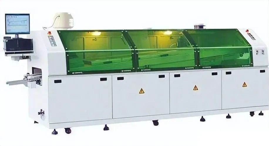
5) Warpage caused by improper storage
During the storage of PCBs in the semi-finished stage, they are generally firmly inserted on shelves, and the tightness of the shelves is not adjusted properly, or the stacking of boards during storage can lead to mechanical deformation of the boards.
This is especially serious for thin boards below 2.0mm.
3. Engineering Design Causes
1. Uneven copper surface area on the circuit board, with more on one side and less on the other. In areas with sparse lines, the surface tension is weaker than in dense areas, and excessive heat can cause warpage.
2. Due to special media or impedance relationships, the laminated structure may be asymmetric, leading to warpage.
3. The hollow positions on the board are too large and numerous, making it easy to warp at high temperatures.
4. Too many panels on the board, with hollow spaces between the panels, especially rectangular boards, are also prone to warpage.
5. How to Improve PCB Warpage?
1. Precautions During PCB Design
1) Copper pouring within the board to increase surface tension.
When the board is longer than 80mm without copper and the thickness is less than 1.0mm, it can lead to warpage.
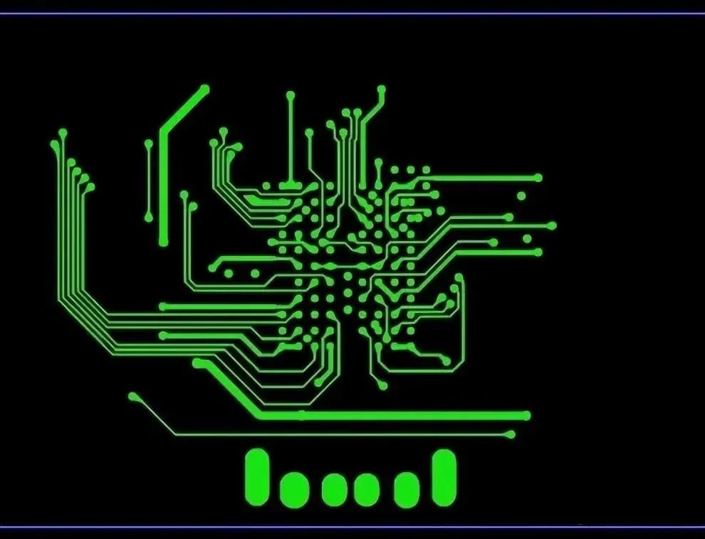
Before Copper
If the board cannot be pressed together and cannot be thickened, heavy pressing of the warped board is used.
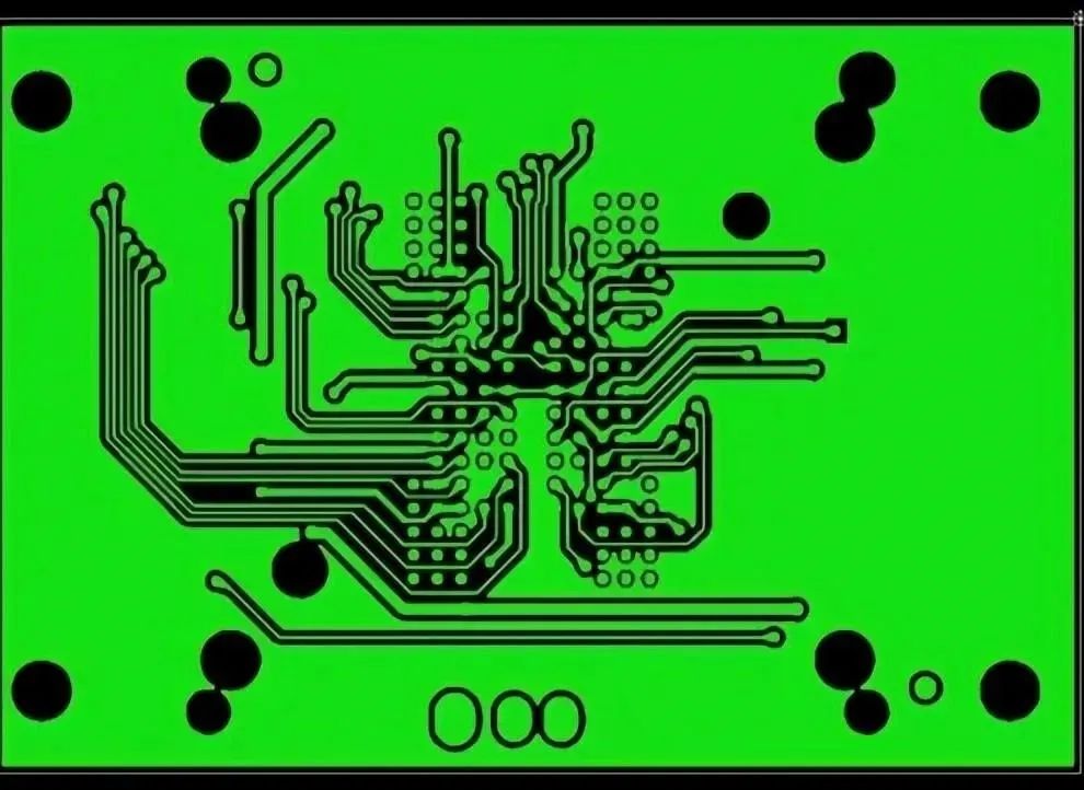
After Copper Plating
2) Copper plating in hollow areas, adding processes
When there are too many hollow positions on the board and the board is too large, it is easy to bend after reflow soldering.
During the PCB manufacturing process, all dielectric layers are distributed evenly. However, it is the uneven distribution of copper layers that leads to PCB warpage. To prevent warpage, design engineers must balance the copper patterns on each layer of the circuit board with the circuit area. Design engineers must also balance component layouts, assembly distributions, and thermal distributions to reduce warpage.
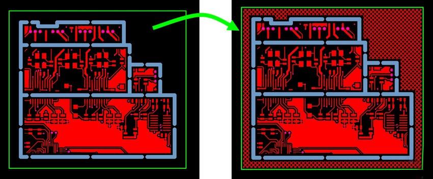
Copper Plating in Hollow Areas, Adding Processes
For example, if the outer top surface has a large copper surface while the outer bottom surface has very few copper traces, the PCB will have a greater tendency to warp after etching. Design engineers must ensure that the pattern area of the two outer layers matches as closely as possible. If there is a significant difference in copper area between the two sides, it is advisable for the designer to add a separate copper mesh on the thinner side to balance both.
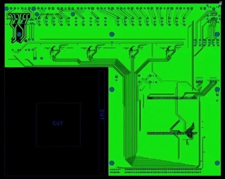
Before Copper Plating
Recommendation: Copper plating in hollow areas to reduce board warpage; additionally, if the internal structure does not affect functionality, copper should also be poured; the last recommendation is to process edges while pouring copper.
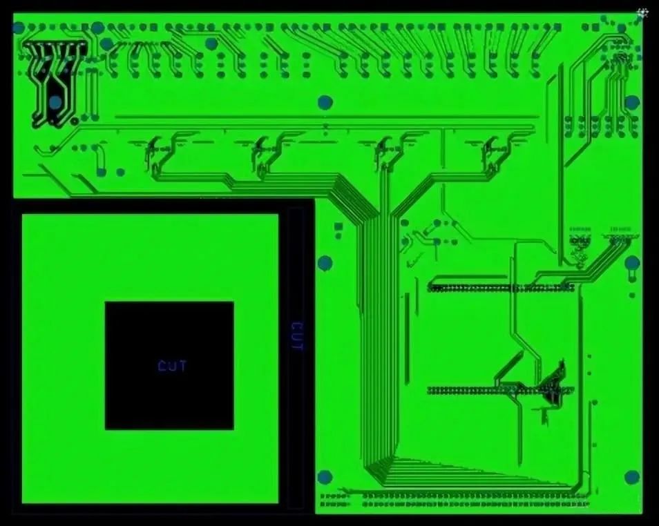
After Copper Plating
3) Ensure that the core board and PP board are of the same brand
The core board and PP board of multilayer boards must be of the same brand; otherwise, the board will warp.
For example, in a 6-layer board, if the PP sheet is asymmetric: the PP sheet of layers 2-3 is thin, while the PP sheet of layers 4-5 is thick, this will cause warping when pressed. Therefore, the core board and PP sheets must be of the same brand to ensure consistent thickness and to maintain the symmetry of the multilayer board PP sheets.
4) Maintain symmetry in the arrangement of prepreg layers
Manufacturers must ensure that the arrangement of interlayer prepreg is symmetrical. For example, for a six-layer board, the thickness between layers 1-2 and 5-6 should ideally be the same, including the number of prepreg sheets. This will prevent warpage after lamination.
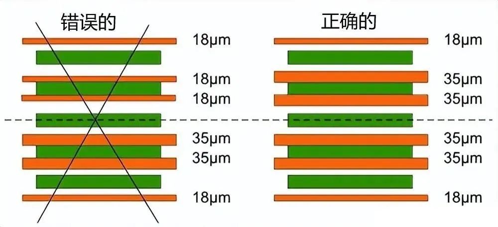
Maintain Symmetry in the Arrangement of Prepreg Layers
2. Precautions During PCB Processing
1) PCB Before Cutting
Before cutting the copper-clad board, the PCB should be baked (150°C, time 8±2 hours) to remove moisture from the board and ensure that the resin in the board is completely cured, further eliminating residual stress in the circuit board, which is useful for preventing warpage.
Currently, many double-sided and multilayer boards still adhere to the baking step before or after cutting. However, some board factories have exceptions. The baking time in PCB factories also varies, ranging from 4 to 10 hours. It is recommended to decide based on the grade of the printed circuit board produced and the customer’s requirements for warpage.
Both methods of baking the entire board before cutting or after cutting are feasible. It is recommended to bake the board after cutting, and the inner boards should also be baked.
2) The Longitude and Latitude of the Prepreg
After the prepreg is bonded, the shrinkage rates in the longitude and latitude directions are different. It is essential to distinguish between longitude and latitude during the cutting and bonding process; otherwise, it may easily lead to warpage of the finished board after bonding, even if pressure is applied to the baked board, it is difficult to correct.
The causes of warpage in multilayer boards are often due to the lack of distinction in longitude and latitude of the prepreg during lamination and random stacking.
How to distinguish between longitude and latitude? The rolling direction of the prepreg is longitudinal, while the width direction is latitude; for copper foil boards, the long side is latitude, and the short side is longitudinal. If unsure, you can consult the manufacturer or supplier.
3) Stress Relief After Bonding
After multilayer boards undergo hot and cold pressing, they should be removed, cut, or milled to remove burrs, and then laid flat in an oven at 150°C for 4 hours to gradually release internal stress and allow the resin to cure completely; this step cannot be omitted.
4) Thin Boards Need to be Straightened During Plating
For ultra-thin multilayer boards of 0.4 to 0.6mm used for surface plating and pattern plating, special clamping rollers should be made. After clamping the thin board on the automatic plating line, use a round rod to clamp the entire clamping roller. String the rollers together to straighten all the boards on the roller, ensuring that the plated boards do not deform.
Without this measure, the boards will bend after plating a copper layer of 20 to 30um, making it difficult to remedy.
5) Cooling After Hot Air Leveling
During hot air leveling of PCBs, they are affected by the high temperature of the solder tank (about 250°C). After removal, they should be placed on a flat marble or steel plate to cool naturally before being sent to the post-processing machine for cleaning, which is beneficial for preventing warpage of the circuit board.
Some factories immediately place the boards in cold water after hot air leveling to improve the brightness of the lead-tin surface, then take them out for post-processing a few seconds later. This thermal shock may cause certain types of circuit boards to warp, leading to twists, delamination, or bubbling.
Additionally, gas flotation beds can be installed on equipment for cooling.
6. PCB Warpage Repair Methods
1. Repairing PCB Warpage During PCB Processing
During PCB processing, boards with significant warpage are selected and flattened using a roller leveling machine before entering the next process. Many PCB manufacturers believe this practice is effective in reducing the warpage rate of finished PCB boards.
2. Repairing Warpage of Finished PCB Boards
For finished products, if the warpage exceeds the limit and cannot be flattened using a roller leveling machine, some PCB factories place them in a small press (or similar fixture) to press the warped PCB board, leaving it for several hours to ten hours for cold pressing. From practical application, this method does not show significant results. Firstly, the flattening effect is minimal, and secondly, the flattened boards are prone to rebound (i.e., warpage recovery).
Some PCB factories heat the small press to a certain temperature before performing hot pressing on the flattened PCB boards, which yields better results than cold pressing. However, excessive pressure may lead to deformation of the wiring; if the temperature is too high, it can cause defects such as discoloration of the rosin. Moreover, whether cold pressing or hot pressing, it takes a long time (several hours to over ten hours) to see results, and the rebound rate of flattened PCB boards is also high.
Here, the method of hot stamping with a bow-shaped mold for flattening is recommended. Depending on the area to be flattened, simple bow-shaped molds are used (see Figure 1). Two types of leveling operations are proposed here.
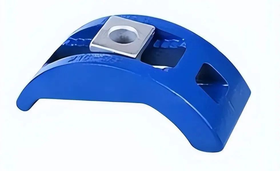
1) Clamping the warped PCB board into the bow-shaped mold and baking for leveling:
The warped PCB board is bent facing the curved surface of the mold, and the fixture screws are adjusted to make the PCB board deform in the opposite direction. Then the mold with the PCB board is placed in the oven and heated to a certain temperature for baking. Under heating conditions, the stress in the substrate gradually relaxes, and the deformed PCB board returns to a flat state. However, the baking temperature should not be too high to avoid discoloration of the rosin or yellowing of the substrate. But the temperature should not be too low, as it requires a longer time to fully relax the stress at lower temperatures.
Generally, the glass transition temperature of the substrate can be used as a reference temperature for baking. The glass transition temperature is the phase change point of the resin, at this temperature, polymer chain segments can rearrange, allowing the substrate stress to relax fully.
Since the flattening effect is significant, the advantage of using a bow-shaped mold for flattening is that the investment is minimal. Ovens can be obtained in PCB factories. The leveling operation is very simple. If there are many warped boards, making several bow-shaped molds is sufficient. They can be placed in the oven at once. If there are fewer molds, the drying time is shorter (around tens of minutes), making the flattening work more efficient.
2) Clamping the PCB board after softening into the bow-shaped mold for flattening:
For PCB boards with relatively minor warpage, the boards to be flattened can be placed in an oven that has been heated to a certain temperature (the temperature setting can refer to the glass transition temperature of the substrate). The substrate is baked in the oven for a certain time, and the softening condition is observed. Generally, the baking temperature for fiberglass cloth substrates is higher, while the baking temperature for paper-based boards can be lower; thicker boards can be baked at slightly higher temperatures, and thinner boards can be baked at slightly lower temperatures.
PCB boards sprayed with rosin should not be baked at excessively high temperatures. After baking for a certain time, take a few to a dozen boards, clamp them into the bow-shaped mold, adjust the pressure screws, and make the PCB board slightly warped in the opposite direction. After the board cools and sets, the mold can be removed, and the flattened PCB board can be taken out.
Bow-shaped mold flattened PCB boards have low warpage; even after wave soldering, they can basically maintain a flat state; the impact on the appearance color of the PCB board is also minimal.
PCB warpage is a headache for PCB manufacturers. It not only reduces yield but also affects delivery time. If the bow-shaped mold is used for hot flattening, and the flattening process is reasonable and suitable, it can flatten warped PCB boards and solve delivery time issues.
Above is a brief introduction to PCB warpage, its causes, and solutions. I hope it will be useful to everyone, and I welcome everyone’s guidance.
Copyright Notice: This article’s copyright belongs to the original author and does not represent the association’s viewpoint. Articles promoted by the “Jiangxi Province Electronic Circuit Industry Association” are for sharing purposes only and do not represent the stance of this account. If there are copyright issues, please contact us for deletion.