1. IntroductionPower optimization for FPGAs is a systematic project that requires collaborative optimization from multiple levels including design architecture, RTL code, tool configuration, and physical implementation, while balancing performance, area, and power consumption (PPA). For Zynq/MPSoC, which also includes the PS side, there are more factors to consider and more methods to apply. For example, a recent customer in the ProAV industry used the ZU4EV platform, which includes both the PS system, streaming media processing, and the PL side with HDMI/SDI transceivers, algorithm processing, and applications such as VCU 4K encoding and decoding. Due to the mobile and portable business scenarios, there is a sensitivity to power consumption and heat generation. Through a series of optimization measures, a power saving of nearly 2W was ultimately achieved.2. Thermal Design Process
Thermal design for AMD FPGAs is a key aspect to ensure device stability, extend lifespan, and optimize power consumption. The thermal characteristics of FPGAs are closely related to their power consumption, package type, ambient temperature, and cooling solutions in comprehensive design for application scenarios.
A complete power/thermal management/board-level design methodology is illustrated in the following diagram:
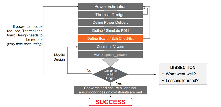
AMD provides various tools for power assessment, thermal modeling, etc.
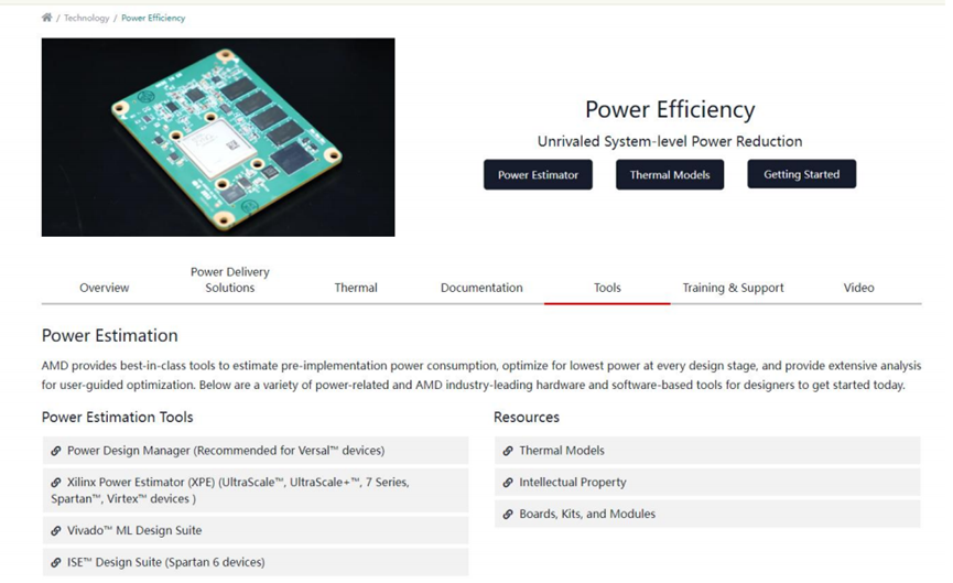
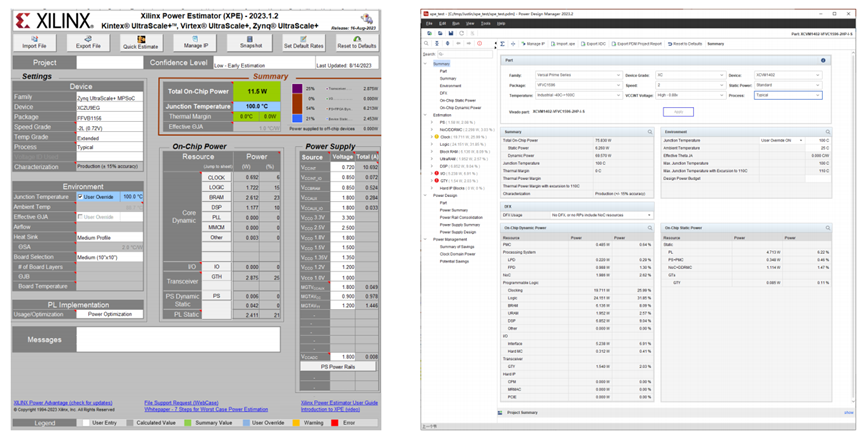
Power assessment tools:
Refer to the official documentation:XAPP1377: Designing Heatsinks and Thermal Solutions for Xilinx Devices which details the steps for designing thermal systems, including:
A. Determine the type of package lid and related documentation.
B. Determine the contact area and height requirements of the package.
C. Design the heatsink base.
D. Design the heatsink fins and airflow direction (for liquid cooling, this would be fluid flow).
E. Design the correct peripheral accessories.
F. Select the best thermal interface material (TIM) and determine the application. TIM is the material that improves thermal contact between the device and the thermal stack.
G. Determine the thermal parameters for simulation and validate the thermal design.
H. Determine the correct assembly, testing, and debugging (if necessary)..
3. Device SelectionAMD main chips offer various compatible package models, such as speed grades-1,-2,-3, industrial grade, commercial grade, etc. Taking XCZU4EV-2SFVC784I as an example, if you choose XCZU4EV-L2SFVC784E as a substitute (L stands for Low Power), it can reduce the core voltage to save some power consumption.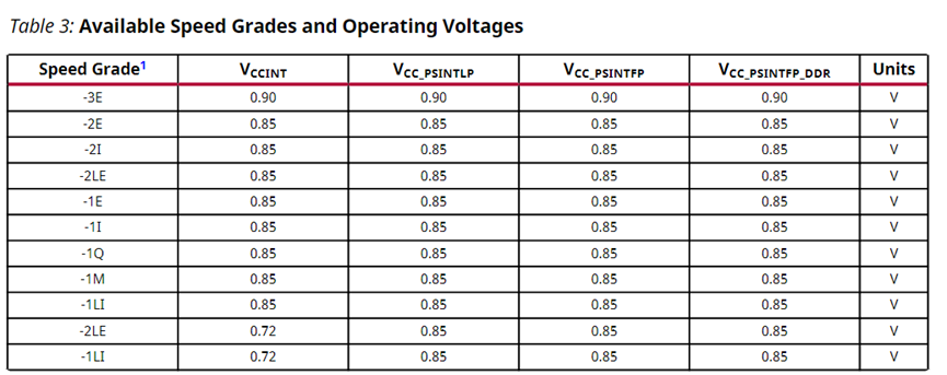
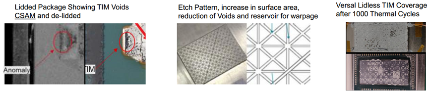
In terms of packaging, choosing Lidless Packaging can also have advantages for heat dissipation.
Uncapped devices have better thermal performance because their RJC (Thermal Resistance from Junction to Case) value is lower. Compared to capped devices, they have lower junction temperatures;
this improves the efficiency of thermal solutions; reduces static power consumption or allows for higher operating ambient temperatures.
For other peripheral device selection, try to simplify or choose low-power devices.
For example, in the design of DDR, under the condition of meeting bandwidth requirements, use LPDDR4 to replace DDR4. LPDDR4 generally saves power consumption by 30%~50% compared to DDR4 under the same bandwidth, especially advantageous in light load and standby scenarios. This is also the core reason for its replacement of DDR4 in mobile devices, edge computing, and low-power embedded systems.
4. PS Side Optimization Measures
The MPSoC PS side adopts a multi-power domain design, which can reduce static power consumption by shutting down or lowering the frequency of idle domains:
PS_VCC: Core processors (A53, R5) and logic circuits.
PS_VCCIO: I/O interfaces (such as GPIO, UART, SPI) power supply.
PS_VCC_PLL: PLL clock power supply.
PS_VCC_DDR: DDR/LPDDR controller power supply.
Idle domain power can be shut down through the PMU (Power Management Unit) or external power management chips (such as PMIC), for example: if the R5 processor is not used, its power domain can be shut down (configured through the power management registers of PS); unused I/O Bank (such as unconnected peripheral GPIO groups) can have their corresponding PS_VCCIO power supply shut down.
Processor core switching and frequency reduction can also significantly save power, A53 supports symmetric multiprocessing (SMP), and can shut down some cores under light load; reduce the clock frequency of A53/R5; enable processor idle states (such as ARM‘s WFI/WFE instructions), allowing cores to enter low-power modes.
Peripheral optimization: for example, DDR frequency reduction; PHY chips (such as Ethernet PHY, HDMI PHY, etc.) can shut down transceivers when idle.
For the application layer, reduce processor occupancy: avoid infinite loops and busy waiting, use interrupts or event-driven instead of polling; data localization: place frequently accessed data on-chip RAM (such as A53‘s L2 cache), reducing access times to DDR, etc.5. PL Side Optimization Measures
Clock Network Optimization (the main source of dynamic power):
Utilize Xilinx dedicated clock gating units (such as BUFGCE, LUT-based gate) to turn off clocks for idle modules. For example, use BUFGCE to control the distribution of high-frequency clocks.
Clock Frequency and Division:
Allocate the minimum necessary frequency according to module requirements: non-critical paths (such as low-speed interfaces, state machines) use divided clocks to avoid “one clock fits all“. For example, use MMCM to generate multiple frequency levels (100MHz for core logic, 25MHz for peripheral interfaces).
Avoid over-designing clock frequencies: if timing analysis shows significant slack, the clock frequency can be reduced (for example, from 200MHz to 180MHz, dynamic power decreases linearly with frequency.
Merge clocks, minimize the use of MMCM, as each MMCM may consume around 100mw of power on the MSoC.
IO Driving:
A. Under the premise of meeting performance, reduce IO driving current through constraints, for example, change from 12ma to 8ma;
set_property DRIVE 8 [get_ports {data_out}];
B. Change the IO driving slew rate to slow
set_property SLEW SLOW [get_ports {data_out}].
Reduce Clock Buffers and Fanout:
Avoid unnecessary global clock buffers (BUFG): local clocks (such as divided clocks within small modules) can use regional buffers (BUFR), reducing global wiring load.
Split high fanout clocks: if a clock drives a large number of registers, the clock tree can be split into multiple subtrees (through multiple BUFGCE), controlling enables separately to reduce clock load.
Resource Reuse:
Multiple modules share a single DSP48 (such as time-division multiplexed multipliers), reducing the number of resource instances (the more resources, the higher the static power); small capacity storage should prioritize using BRAM (block RAM) instead of distributed RAM made of LUT, as BRAM has lower power density (power consumption/bit) and more concentrated wiring.
Transceiver Swing:
For example, if a customer uses 12G-SDI, under good signal conditions with short traces, it is possible to save some dynamic power by reducing the swing. When the swing is reduced from 800mV to 400mV, the Tx end driving power can be reduced by about 40%~60% (as current decreases linearly with swing, power consumption decreases approximately linearly).SDI transceiver swing can be controlled through the txdiffctrl_in port.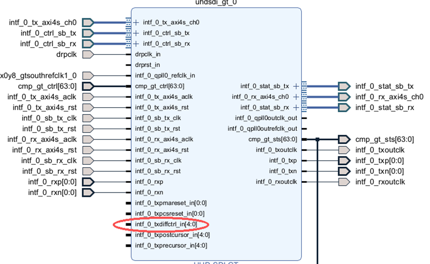
6. Vivado Tool Optimization Measures
Synthesis Stage Optimization
The synthesis stage converts RTL code into gate-level netlists, and reasonable configuration of synthesis strategies can reduce redundant logic and optimize resource utilization, laying the foundation for subsequent implementation stages.
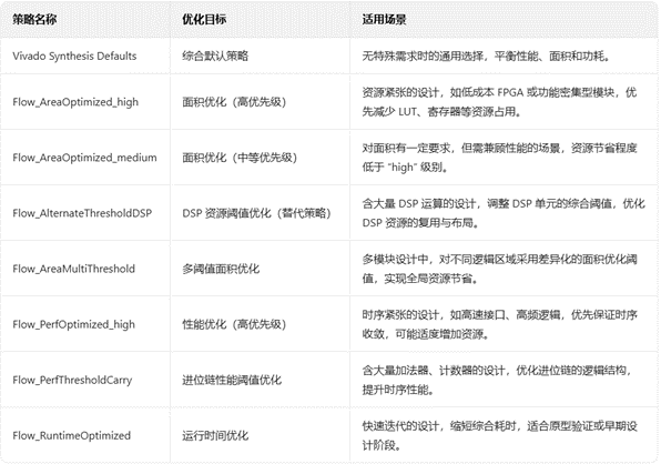
Vivado provides preset synthesis strategies optimized for different targets (power consumption, performance, area):
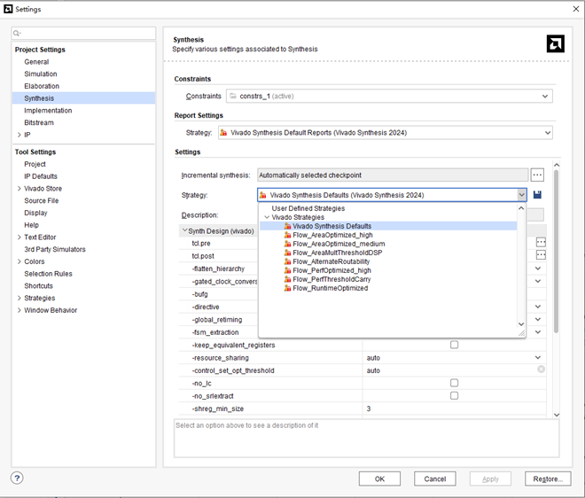
Select the most suitable strategy based on the design.
Implementation Stage Optimization
The implementation stage (including placement and routing) directly affects physical performance (timing, power consumption, routing length) and is the core of optimization. The synthesis stage provides more strategy options, allowing for the selection of Power-related optimization strategies.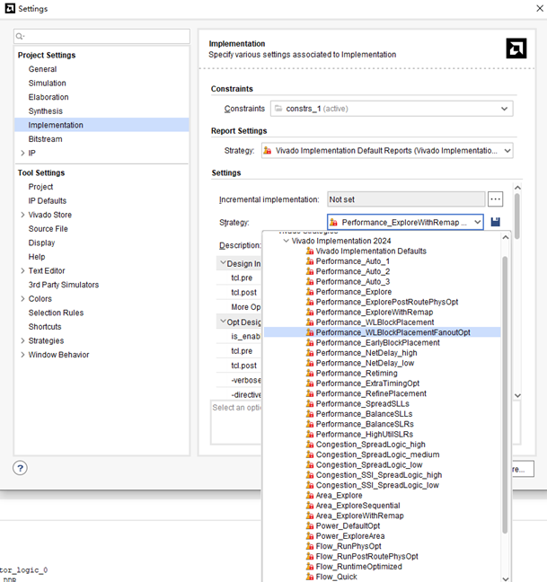
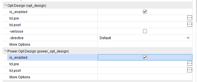
Opt Design (Logic Optimization)
Perform logic-level optimization on the design, including logic retiming, resource sharing, and redundant logic removal, laying the foundation for subsequent placement and routing.-directive set to Default is a general optimization strategy, which can be switched to corresponding specialized strategies (such as AreaOptimized, PerfOptimized, etc.) based on design goals (such as performance, area, power consumption).
Power Opt Design (Power Optimization)
Specifically optimize for power consumption by adjusting logic structures, reducing signal toggle rates, etc., to lower dynamic and static power consumption.is_enabled checked indicates that the current design has enabled the power optimization process, which will allow the tool to add power-driven algorithms during the logic optimization phase to minimize power consumption while meeting timing. This configuration is suitable for power-sensitive FPGA designs (such as battery-powered devices, edge computing scenarios), achieving a good balance between performance and power consumption by enabling both general logic optimization and specialized power optimization.
The final timing status will also have a significant impact on power consumption. By jointly analyzing Vivado‘s report_power and report_timing, locate modules that are “high power and sufficient timing slack” and relax timing constraints or optimize logic structures for them. For example, if a module has a timing slack of 10ns and a power consumption ratio of 15%, reducing its clock frequency or increasing gating can reduce power consumption. In general, avoid excessive timing constraints, set frequencies and path delays according to actual needs; partition clock domains for different modules, using high-frequency clocks only for critical paths and low-frequency clocks for non-critical modules;
Through this collaborative design, it is possible to achieve reduced power consumption while ensuring performance.
Reference Documents:
1. AMD Technical Expert Li Jinhua “High-reliability Hardware Design”.
2. AMD Technical Expert Gu Yongguo “Power reduction”.
If you have any questions related to FPGA power optimization, please feel free to contact: