Today, we summarize the latest research findings on advanced smartphone SoC packaging technology, revealing how packaging technology is reshaping the development trajectory of mobile processors.
Market Landscape: Dominated by Three Major Players, Diverging Technology Paths
The smartphone application processor (APU) market is dominated by Qualcomm, Apple, and MediaTek, collectively holding over 80% of the market share. However, it is concerning that the overall smartphone APU market is expected to remain stagnant in the coming years.
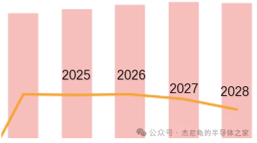 Smartphone APU Market Volume
In terms of packaging technology selection, the market shows a clear stratification: PoP (Package-on-Package) configurations are primarily aimed at luxury and high-end smartphones, while mid-range and low-end smartphone APUs adopt cost-effective flip-chip chip-scale packaging (FC CSP) configurations. This divergence in technology paths reflects the different trade-offs between performance and cost for products at various price points.
Fan-Out Packaging: A New Choice for High-End Smartphones
Significant Technical Advantages
Fan-out packaging technology is becoming an important solution for assembling high-end smartphone SoCs. This technology eliminates the substrate, achieving a thinner package thickness while providing higher interconnection density. Its core advantages include:
(1) Better signal integrity
(2) Excellent thermal performance
(3) Support for over 1000 I/O connections
(4) Features three or more redistribution layers (RDL), with minimum line width/spacing reaching advanced levels
Practical Application Case
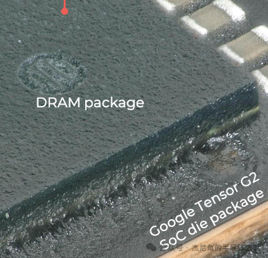
Taking the Google Pixel 7 Pro equipped with the Tensor G2 SoC as an example, this chip utilizes Samsung’s fan-out panel-level packaging (FO-PLP) technology. Disassembly analysis shows:
(1) DRAM packaging is stacked on top of the Google Tensor G2 SoC chip packaging
(2) The entire chip is assembled using PoP technology and then integrated onto the smartphone motherboard
(3) The package contains four LPDDR5X DRAM chips, using gold wire bonding, with a total of 384 wires
Technical Comparison: Innovative Competition Among Four PoP Solutions
A deep comparison of four high-end smartphone PoP technologies:
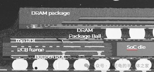
1. Standard PoP vs FO-PLP PoP
Standard PoP uses solder balls as interconnections between the upper and lower substrates, while FO-PLP PoP replaces solder balls with a PCB frame, solving the ball deformation issue. The minimum line width/spacing of FO-PLP’s RDL is 7/10µm, significantly better than the 15/15µm of standard substrates.
2. MCeP vs FO-PLP
MCeP uses copper core solder balls for interconnection, while FO-PLP’s PCB frame uses less copper material and has no deformation issues. Although the height of the PCB frame is 100µm greater than that of copper core solder balls, it can integrate thicker SoC chips, providing better mechanical reliability.
3. InFO vs FO-PLP
Apple’s InFO packaging uses TIV as the interconnection between DRAM packaging balls and RDL, while FO-PLP’s PCB frame not only provides connection functionality but also allows for additional routing around the chip, offering greater design flexibility in PoP configurations.
Cost Analysis: Economic Considerations of Technology Upgrades
Despite the significant performance advantages of fan-out packaging technology, cost factors remain an important consideration. Analysis shows that there are significant differences in the average selling prices of different packaging types:
(1) Flip-chip PoP (FC PoP) and flip-chip CSP (FC CSP) are lower in cost
(2) Fan-out PoP (FO PoP) is higher in cost but provides a value-equivalent performance boost for high-end devices
The cost breakdown for the Google Tensor G2 SoC shows that raw material costs account for 53% of the front-end wafer cost, yield loss costs account for 18%, and labor costs account for 26% of the packaging manufacturing price.
Future Outlook: Chiplets and 3D Stacking Technology
As Moore’s Law approaches physical limits, fan-out packaging technology is evolving towards more innovative directions:
(1) Chiplet design will become an important trend, achieving chip partitioning through fan-out RDL interconnections
(2) 3D stacking technology will adopt advanced processes such as TSV + micro-bumps or hybrid bonding
(3) Lateral integration and 3D stacking will develop in parallel to meet the needs of different application scenarios
Major manufacturers like TSMC and Samsung, along with OSAT companies, are actively developing various solutions to drive packaging technology towards higher density and performance.
In conclusion:
The packaging technology for smartphone SoCs is undergoing a significant transformation from traditional to innovative approaches. Fan-out packaging technology not only meets the stringent requirements of high-end smartphones for performance, thermal management, and thickness but also lays a solid foundation for future chiplet and 3D integration technologies. As technology continues to mature and costs are optimized, we have reason to believe that advanced packaging technology will continue to play a key role in pushing the boundaries of mobile computing performance.
For more details, please follow Knowledge Planet.