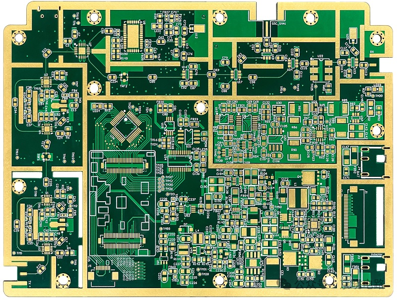
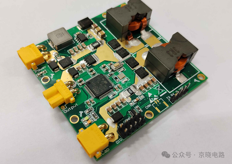
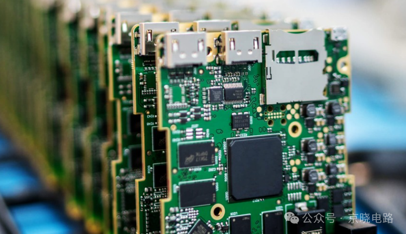
In the field of electronic device manufacturing, printed circuit boards (PCBs) are undoubtedly a critical component, and their surface treatment processes have a profound impact on the performance, reliability, and production costs of PCBs. From consumer electronics such as smartphones and tablets to industrial control devices, automotive electronic systems, high-end communication equipment, and aerospace instruments, different application scenarios have varying requirements for PCB surface treatment processes. Therefore, gaining a deep understanding and making informed choices regarding PCB surface treatment processes has become a crucial aspect that electronic engineers and manufacturers must prioritize during product design and production.
Basic Types of PCB Surface Treatment Processes
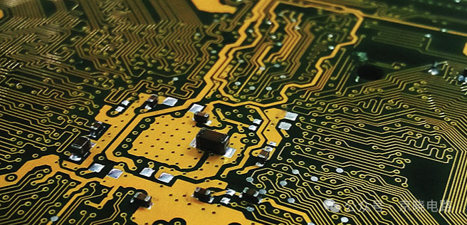
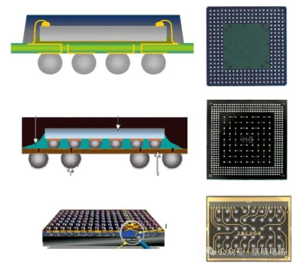
Common PCB surface treatment processes are diverse and mainly include Hot Air Solder Leveling (HASL, which includes leaded and lead-free soldering), immersion tin, immersion silver, Organic Solderability Preservative (OSP), Electroless Nickel Immersion Gold (ENIG), Electroless Nickel Electroless Palladium Immersion Gold (ENEPIG), and Electroplated Nickel Gold (hard gold and soft gold). Each of these processes has unique characteristics and plays a key role in different application scenarios. In domestic PCB manufacturing, the main surface treatment processes used are immersion gold, leaded soldering, and lead-free soldering. Below, we will mainly introduce these three common processes.
 01
01
Immersion Gold (ENIG) Process
The immersion gold process deposits a nickel layer and a gold layer on the copper surface of the PCB through a chemical displacement reaction. The nickel layer thickness is generally between 3 – 6μm, serving as a barrier to the copper and is the actual surface for component soldering; the gold layer thickness is 0.05 – 0.1μm, primarily to prevent oxidation of the nickel layer during storage.
Advantages: The immersion gold process offers extremely high surface flatness, making it particularly suitable for soldering fine-pitch pins and small solder points of components, meeting the assembly requirements of high-density PCBs. Additionally, it has excellent solderability and long-term storage stability, allowing for multiple reflow soldering without significant decline in solderability. Furthermore, the immersion gold process can serve as a high-quality substrate for Chip-On-Board (COB) wire bonding.
Disadvantages: Its cost is relatively high, mainly due to the expensive price of gold and the complexity of the process. Moreover, when using a non-electroplated nickel process, there is a risk of black pad issues, and the nickel layer may oxidize over time, which can impact the long-term reliability of the product.
Applicable Scenarios: Commonly used for boards with high requirements for surface connection functionality and storage period, such as the button area of mobile phones, edge connection areas of router housings, and electrical contact areas of chip processor flexible connections. The immersion gold process is also widely used in high-end communication devices, aerospace, and military electronic equipment, where the requirements for electrical performance and reliability are extremely stringent, and the immersion gold process can effectively meet these needs.
 02
02
Leaded Soldering Process
The leaded soldering process involves immersing the circuit board in molten tin-lead alloy solder, allowing the solder to cover the exposed copper surfaces of the PCB, and then using high-pressure hot air to blow away excess solder to achieve a flat surface.
Advantages: It is relatively inexpensive and has good soldering performance, forming strong solder joints with various electronic component pins. Additionally, leaded solder boards exhibit excellent mechanical strength and brightness.
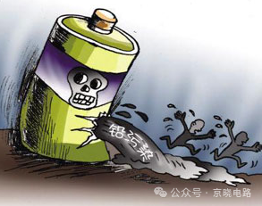
Disadvantages: Due to the presence of lead and other heavy metals, it poses significant environmental hazards, does not comply with environmental standards, and cannot pass ROHS testing. Furthermore, the surface flatness of soldered boards is inadequate, making it unsuitable for soldering fine-pitch pins and very small components. During PCB processing, solder beads may easily form, potentially causing short circuits in fine-pitch pin components. In double-sided SMT processes, during high-temperature reflow soldering of the second side, the solder may easily remelt, forming solder beads or ball-shaped solder points, further affecting surface flatness and soldering quality.
Applicable Scenarios: It still has certain applications in products with lower environmental requirements, strict cost control, and less demanding soldering precision, such as some traditional consumer electronics and low-end industrial equipment. However, with the increasing strictness of environmental requirements, the application range of leaded soldering processes is gradually shrinking.
 03
03
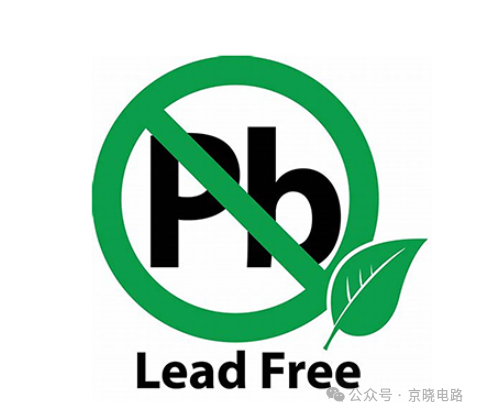
Lead-Free Soldering Process
The lead-free soldering process operates on principles similar to leaded soldering, but uses lead-free tin alloy solder to meet environmental requirements.
Advantages: It has good soldering performance, strong solderability, and can meet the soldering needs of most electronic components. Additionally, it complies with environmental standards and can pass ROHS testing.
Disadvantages: Its brightness is slightly duller compared to leaded soldering. It also suffers from poor surface flatness, making it unsuitable for soldering fine-pitch pins and small components, and is prone to solder beads. In double-sided SMT processes, it also faces issues with solder beads and surface irregularities. Furthermore, the lead-free soldering process requires higher equipment and process control, resulting in higher costs compared to leaded soldering.
Applicable Scenarios: It is widely used in various electronic products with strict environmental requirements, such as consumer electronics, automotive electronics, and medical devices. In these fields, products need to comply with relevant environmental regulations, making lead-free soldering processes an important choice to meet soldering needs and environmental requirements.
Factors to Consider When Choosing PCB Surface Treatment Processes
01
Requirements for Pad Flatness
If there are large BGAs or high-precision components with smaller spacing on the PCB, the requirements for pad flatness are extremely high. In this case, the immersion gold (ENIG) process, which can provide an extremely flat surface, becomes the ideal choice; the Organic Solderability Preservative (OSP) process, which forms a uniformly thin organic film, has minimal impact on PCB flatness and is also suitable for such scenarios; the Electroless Nickel Electroless Palladium Immersion Gold (ENEPIG) process also has excellent surface flatness and can meet high-precision soldering requirements. In contrast, the soldering process, due to its poor surface flatness, may not meet the soldering requirements for high-precision components, and using it in such cases may lead to soldering defects.
 02
02
Solderability and Wetting Requirements
Solderability is one of the key indicators of PCB surface treatment processes. Both leaded and lead-free soldering processes exhibit excellent solderability, forming strong solder joints with various electronic component pins, and are widely used in products with high reliability requirements. In contrast, the OSP process is relatively weaker in solderability; although it can meet soldering needs under normal circumstances, it may fall short in some scenarios with stringent solderability requirements.
03
Number of Soldering Cycles and Rework Requirements
For PCBs that require multiple soldering or frequent rework, soldering and immersion tin processes perform well. The solder coating of the soldering process is relatively thick, ensuring good soldering performance even if the surface oxidizes; the immersion tin process can maintain good solderability even after multiple thermal shifts. However, the OSP process may not be suitable for multiple soldering and rework situations, as its organic film decomposes during soldering, which can lead to excessive oxidation of the copper surface and reduce soldering quality.
 04
04
Environmental Requirements (RoHS Compliance)
With the increasing awareness of environmental protection and the strict requirements of relevant regulations, RoHS compliance has become an important consideration when choosing PCB surface treatment processes. Processes such as immersion gold (ENIG), immersion tin, immersion silver, and OSP comply with RoHS standards and can be applied in the manufacturing of electronic products with strict environmental requirements. In contrast, the leaded soldering process, due to the presence of lead and other harmful substances, does not meet environmental requirements and has gradually been phased out in areas with high environmental standards.
 05
05
Metal Bonding Requirements
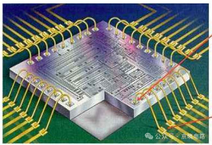
If the PCB requires gold or aluminum wire bonding, processes such as immersion gold (ENIG), Electroless Nickel Electroless Palladium Immersion Gold (ENEPIG), and soft electroplated gold are suitable choices. These processes can provide a good foundation for metal bonding, ensuring reliability and stability. Other processes may not meet the requirements for metal bonding, and using them in such cases may lead to poor bonding quality, affecting product performance.
 Conclusion
The selection of PCB surface treatment processes is a comprehensive consideration of multiple factors. Different processes have their advantages and disadvantages in terms of cost, performance, and environmental protection, making them suitable for different application scenarios. In actual selection, electronic engineers and manufacturers need to weigh the pros and cons of various processes based on specific product requirements, such as pad flatness, solderability, number of soldering cycles, environmental requirements, and metal bonding needs, to make the most appropriate decision.
As electronic technology continues to develop, the requirements for PCB surface treatment processes are also continuously increasing. In the future, process innovation will focus on improving surface treatment quality, reducing costs, enhancing environmental performance, and meeting higher precision soldering needs. For example, developing more advanced immersion gold processes to reduce the occurrence of black pad issues and improve product reliability; exploring new lead-free soldering processes to improve surface flatness and soldering performance; optimizing OSP processes to extend storage life and enhance solderability, etc.
Making informed choices regarding PCB surface treatment processes can not only enhance product quality and reliability but also effectively control production costs, strengthening a company’s competitiveness in the market. In today’s rapidly developing electronics industry, keeping up with process development trends and continuously optimizing process choices is key for electronic engineers and manufacturers to maintain their leading position in the industry.
END Scan to Follow
Focusing on high-speed PCB design, quality assurance
Technical Support: Xiao Jing
 Scan to Follow
Focusing on high-speed PCB design, quality assurance
Jing Xiao Public Account