The development of modern electronic industry is changing rapidly, with large-scale and ultra-large-scale integrated circuits becoming increasingly complex. The traditional method of manually designing and manufacturing circuit boards can no longer meet production needs and is prone to errors. Here, I will introduce how to automatically convert schematics into PCB layouts.
By relying on the editing capabilities of Protel 99 and its powerful automation design capabilities, coupled with a rich component library, it is possible to quickly and effectively draw schematics and convert them into PCB layouts.
01|Setting Component Properties
The electrical schematic is the basis for converting the PCB layout, so it is very important to design the schematic well.
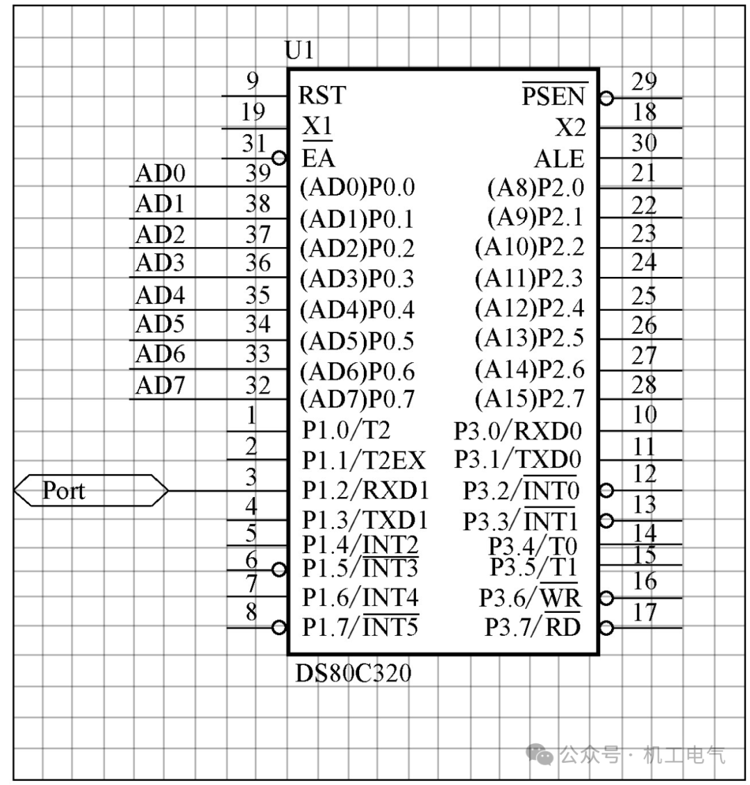
First, adjust the position of all components according to the diagram, then edit the properties of each component one by one. The properties of the components include serial number, package type, pin number definition, etc. Below, we will edit the properties of the component in Figure 1.
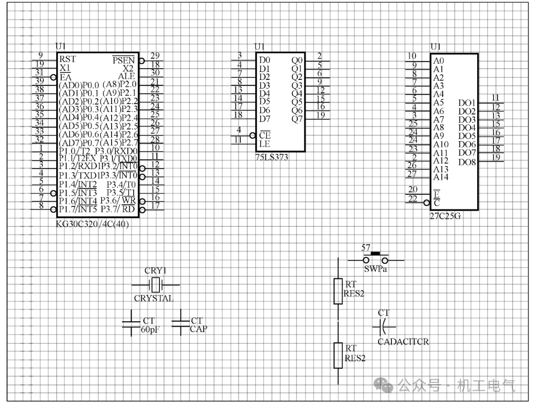
Figure 1 Result after adjusting component positions
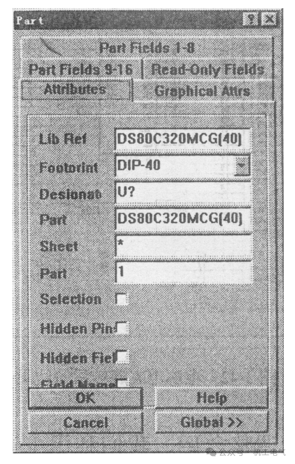
Figure 2 Component property editing dialog box
Set various properties of the components in the dialog box:
1) Lib Ref: Model number from the component library, modification is not allowed.
2) Footprint: Package type of the component, write as “DIP-40”.
3) Designator: Component serial number, write as “U1”.
4) Part Type: Component model, write as “DS80C320 MCG”.
5) Sheet: Drawing number, leave blank for now.
6) Part: Function block serial number, this item is used for multiple identical function blocks, and is invalid for its components.
After setting, click the “OK” button.
Edit all components in Figure 6-1 according to the above method. Here we will set the serial number, model, and package type of the main components as follows:
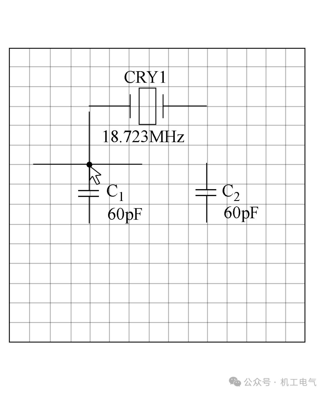
1) Standard Capacitor 1: C1, 60pF, RAD0.2.
2) Standard Capacitor 2: C2, 60pF, RAD0.2.
3) Electrolytic Capacitor: C3, 22μF, RB.2/.4 (PCB library also has .3/.6, .4/.18, .5/.10).
4) Rectifier Diode: DIODE0.4~0.7.
5) Control IC: DIP4, 8, 14, 16, 18, 20, 22, 24, 28, 32, 40, 48, 52, 64, etc.
6) Crystal Oscillator: CRY1, 18, 723MHz, XTL-1.
7) Resistor 1: R1, 200, AXIAL 0.4.
8) Resistor 2: R2, 1K, AXIAL 0.4.
9) Reset Key: S1, SW-PB, RAD0.4.
10) Microcontroller DS80C320MCG (40): U1, DS80C320, DIP-40.
11) Address Latch 74LS373: U2, 74LS373, DIP-20.
12) Program Memory 27C256: U3, 27C256, DIP-28.
1) Click the wire drawing button in the Wring Tools toolbar, after executing the wire drawing command, a cross cursor will appear. Move the cursor to the capacitor C1, a cross with a black dot will appear, as shown in Figure 3. Note, the starting point of the wire must be set on the component pin and a black dot appears, indicating that the electrical connection has been made. All lines connected to the component model must have this black dot.
2) Create the I/O port of the circuit. Based on Figure 1, create the I/O port for the serial interface of the microcontroller 80C320 (pins 3 and 4). Click the port button on the schematic toolbar, then drag the mouse to the appropriate position and click the left mouse button to confirm the I/O port, as shown in Figure 4.
Figure 3 Confirming the starting point of the wire
Figure 4 Confirming the I/O port
03|Generate Netlist from Schematic
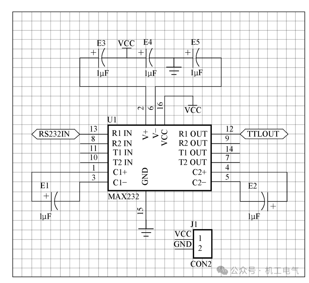
Before making the circuit, we must have the circuit schematic and netlist. We will make a single-sided PCB as shown in Figure 5, all components should be edited according to the component properties mentioned earlier. Next, plan the PCB, according to the schematic plan the size of the circuit, and pay special attention to setting the color of the layers.
Figure 5 Level Conversion Circuit Schematic
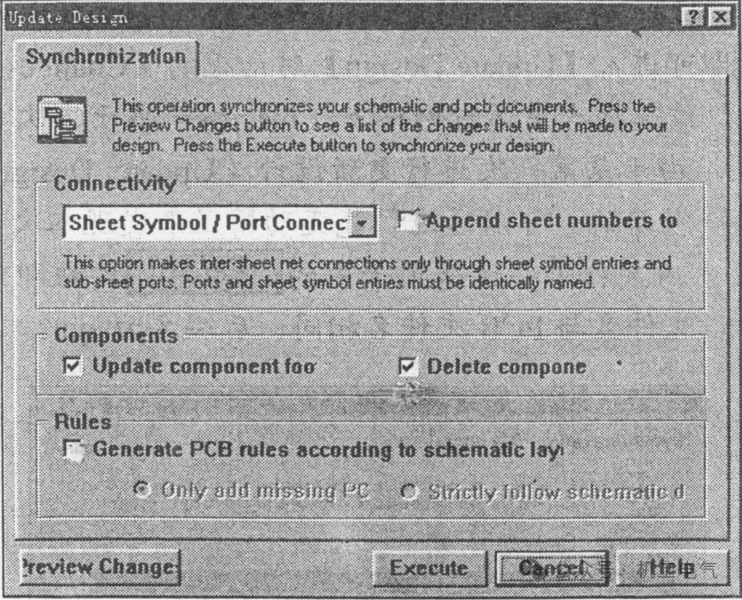
In the schematic editor, execute the command Design/Update and the dialog box shown in Figure 6 will appear, the options in the dialog box are as follows:
Figure 6 “Update Design” Dialog Box
1) Connectivity: Connectivity. Used to select the internal network connection method of the schematic, there are three options: Net Labels and Ports Global, Only Ports Global, and Sheet Symbol/Port Connections, the default is Sheet Symbol/Port Connections.
2) Append sheet numbers to local net name: Append the schematic number to the network name, status is unchecked.
3) Update Component footprint: Update component package number, status is checked.
4) Delete Component if not in netlist: Delete components that are not wired, status is checked.
5) Generate PCB rules according to schematic layout: Generate PCB routing according to the schematic design, status is unchecked.
After clicking the “Preview Change” button, it shows the connections of all components in the design, whether the package is incorrect, and changes the errors found.
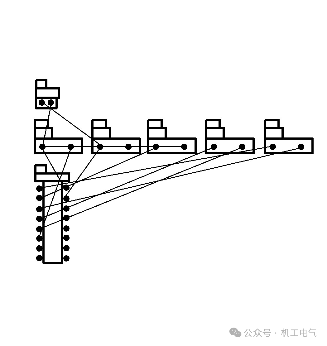
Click the “Execute” button, and the components will be loaded into the netlist and enter the PCB, as shown in Figure 7.
Figure 7 PCB Diagram after Loading Netlist and Components
04|Generate Netlist from Schematic
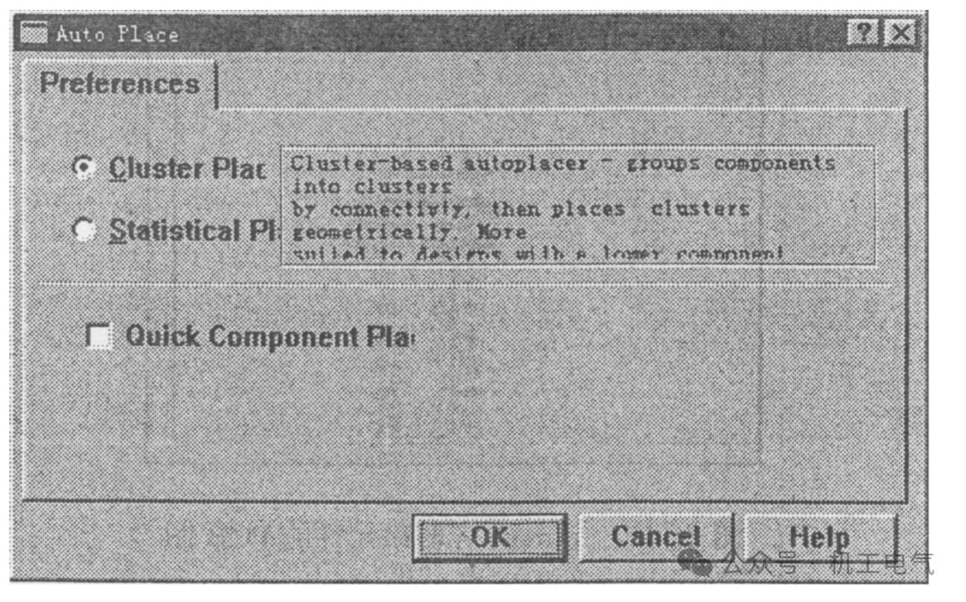
1) In the PCB editor, execute the command Tools/Auto Place and the component auto-layout dialog box shown in Figure 8 will appear. Cluster Placer: Composition layout method, suitable for circuits with fewer components, status is checked, and the other two options are unchecked.
Figure 8 Component Auto-Layout Dialog Box
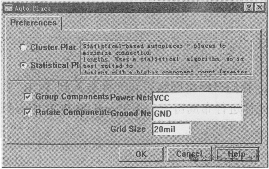
2) Select Statistical Placer with the mouse, and the dialog box shown in Figure 9 will appear. Select Statistical Placer, fill in “VCC” in the “Group…” field, fill in “GND” in the “Rotate…” field, and finally click the “OK” button.
Figure 9 Component Auto-Layout Dialog Box under Statistical Layout
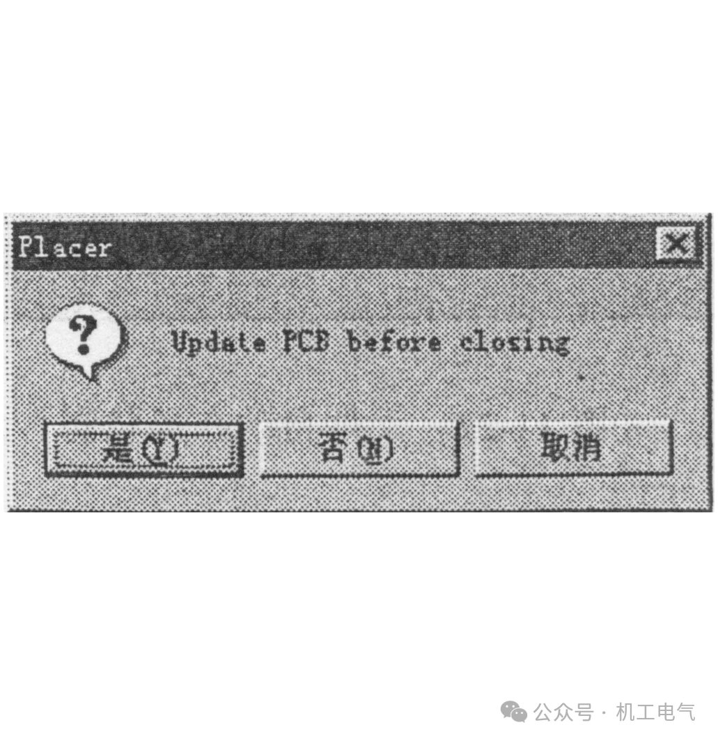
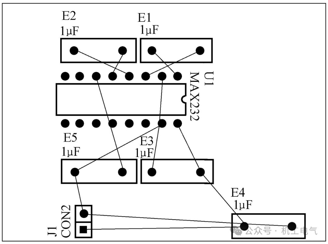
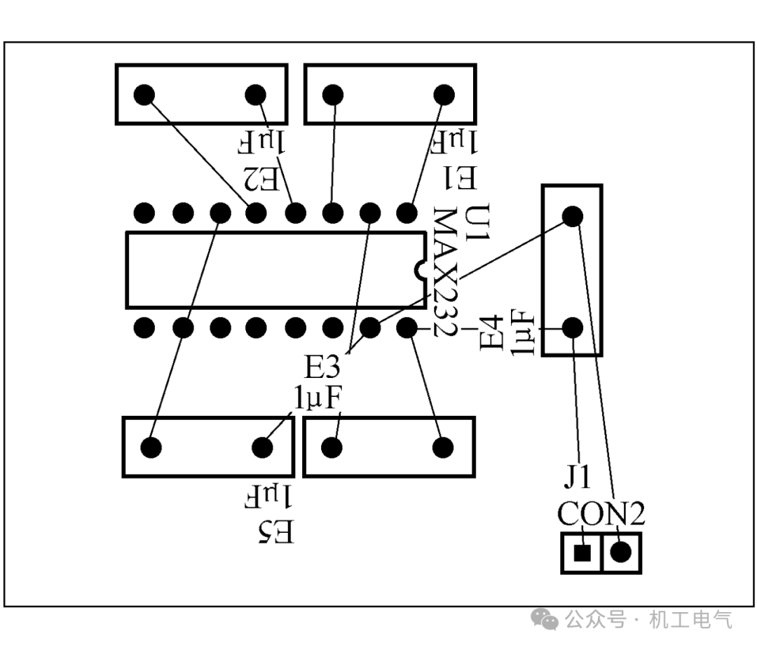
3) Close the auto-layout window, at this point the dialog box shown in Figure 10 will appear, then click the “Yes (Y)” button to show the PCB in Figure 11. After Figure 11 appears, adjust the position of each component, and also modify the PCB frame, ensuring that the connections of each component do not cross. The final result is shown in Figure 12.
Figure 10 Prompt Dialog Box
Figure 11 PCB Diagram after Component Auto-Layout
Figure 12 Final Result of Component Layout
This article is excerpted from “Design and Application of Typical Circuits for New Switching Power Supplies, 3rd Edition”

The book is divided into 7 chapters: Chapter 1 introduces the basic working principles of switching power supplies; Chapter 2 comprehensively describes the characteristics and selection of switching power supply components; Chapter 3 provides detailed descriptions of 6 different power switching power supplies; Chapter 4 introduces the design of power factor correction conversion circuits, listing various design methods for power supply power factor correction circuits; Chapter 5 discusses soft switching technology and power supply efficiency; Chapter 6 elaborates on PCB design technology; Chapter 7 provides answers to some key technologies of switching power supplies, opening the door for power supply developers.
This book focuses on the design of high-frequency transformers for switching power supplies, deeply analyzing the doubts and difficulties of switching power supplies, rich in content, comprehensive in knowledge, fluent in text, and easy to understand. It has high reference value for power supply development engineers and is also suitable for students and teachers in related majors at higher education institutions.
Recommended reading list for enhancing power supply development capabilities:

1、Essentials | AC Motor Control Principles and Control Systems—233-page PPT detailing asynchronous motor control principles and control systems, covering technical needs for students five years after graduation! Automation professionals can learn!
2、“Pulse Power Devices and Their Applications”: Electromagnetic railguns, electromagnetic propulsion, particle beams—these new concept weapons are becoming a reality thanks to pulse power technology!
3、Everything is Numbers: Understanding Differential Equations through Four Real Phenomena!—Reading “Easy to Understand Electrical Mathematics Introduction” makes electrical mathematics really simple.
4、New Book Recommendation: “Energy Storage and Power Market for New Power Systems”, a book that explores the real value of new energy storage based on market-oriented theories and industrial processes!
5、After nineteen years, the “Basic Rules for Power Market Operation” is revised, and major changes are coming to the power market.
6、Essentials | “Tracing Power Electronics” by Professor Chen Wu from Southeast University: History of Power Electronics (48-page PPT available for download).
7、Essentials | Principles and Steps of Lithium-ion Battery Design—Officially compiled by Guoxuan High-Tech, “Power Batteries for Electric Vehicles: From Materials to System Design”, directly facing the opportunities and challenges of the energy transition.
8、[New Book Recommendation] Don’t confuse industrial digitalization with digital industrialization! The differences are significant!
9、Medium to Long-term Energy Storage is entering the “Best Era”, with the book “Medium to Long-term Energy Storage Technology” selected for the National Publishing Fund Project—looking forward to the core demand for new power system development in the next twenty years!
Image and text | Tao Zhe
Editor | Yang Qiong
Reviewer | Fu Chenggui