Documenting work, sharing experiences, and open-sourcing! Speed up!  Committed to ensuring that every step of our design is theoretically supported! Star and follow = progress together.




 Be sure to check the comments section, as some colleagues will discuss and supplement there, enriching this theoretical library together!
Documentation is getting more concise! CPU is burning up 
-
ADC: Analog-to-Digital Converter, converting analog signals into digital signals for processing by digital devices.
-
DAC: Digital-to-Analog Converter, converting digital signals into analog signals for external interfaces.
-
Layout Requirements:
-
Avoid placing the power module near the front-end analog input.
-
Keep the power to load path short to reduce transmission noise coupling.
-
Place high-frequency decoupling capacitors close to the chip power pins.
-
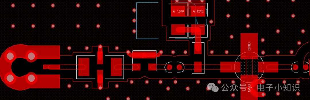
Compact layout for the input front stage.
-
Use a “1” shaped layout, avoiding U-shaped and L-shaped layouts.
-
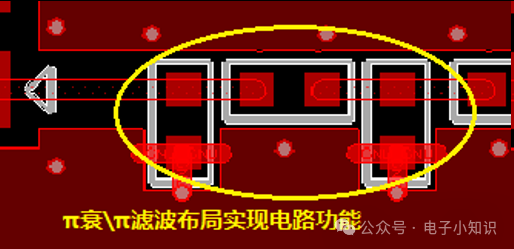
Implement π attenuation and π filtering layout functions.
-
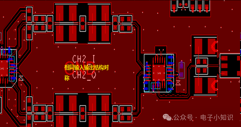
For multiple identical circuit structures, use a symmetrical layout; ensure consistent trace lengths.
Consistency and phase alignment.
-
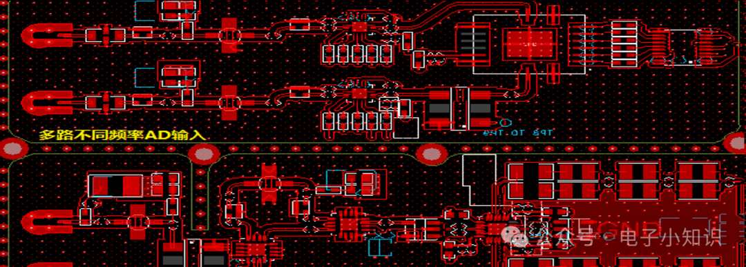
Increase the layout spacing between multiple channels.
-
Add shielding cavities or shielding walls.
-
Wiring Requirements:
-
Minimize loop power splitting.
-
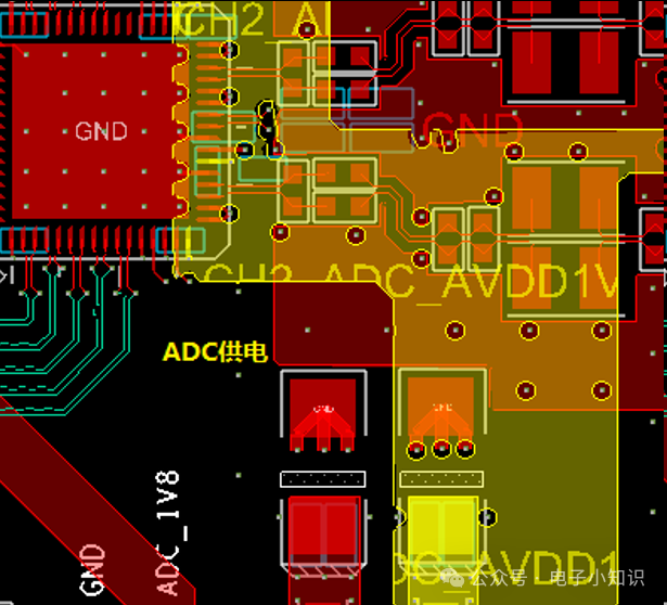
In addition to considering that the analog power layout should not be close to the front-end input, the transmission path should be as short as possible, with minimal loops to reduce power noise introduction.
-
Control attenuation of the shortest analog front stage traces.
-
Minimize wiring length.
-
Control reference impedance in layers, increase wiring width.
-
Use rounded corners and gradual transitions in traces.
-
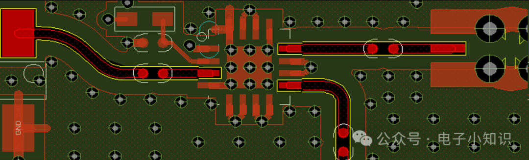
Use layer 2 for cutouts and layer 3 for grounding under the analog area.
-
Impedance Continuity Control – Pad Layer Treatment
-
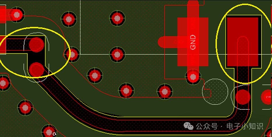
Device pads are the most significant factor for impedance discontinuity in the wiring link; layer isolation can reduce the impedance changes caused by variations in pad and trace width.
Use layer 2 for cutouts and layer 3 for grounding under the analog area.
-
Shielding Ground Treatment
-
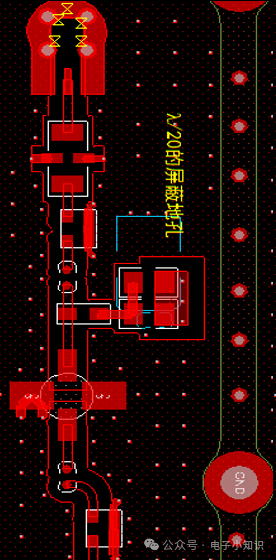
The size of the shielding ground hole spacing determines the amount of EMC radiation leakage; the smaller the distance, the better.
-
Smaller shielding ground hole distances help reduce interference isolation for digital-to-analog and multiple analog front stages, especially when the distance is ≤ λ/20.
-
Analog grounding helps reduce interference, but if the distance is too small, it may increase signal loss; grounding distance should be ≥ 1.5W width.
Cover the analog area with shielding ground and create λ/20 shielding ground holes around the analog traces.
-
Multiple Isolation Treatment
-
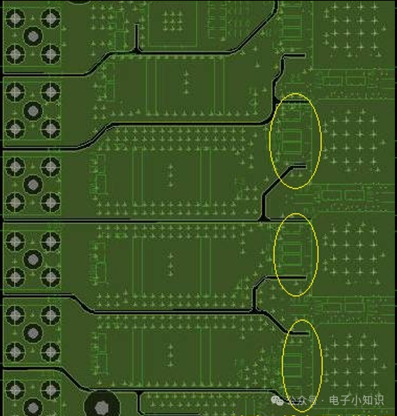
All power and ground planes need to use separation grooves to cut off the noise coupling loops from multiple AD inputs, reducing coupling paths between multiple channels.
-
Digital and Analog Common Ground Treatment
-
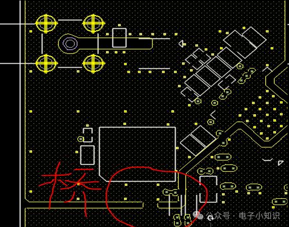
The common ground bridge does not provide a signal return path, only serves as an equipotential short circuit.
-
The width of the bridge should not be too wide, recommended around 60 mils.
-
Use 20-30 mils for isolation grooves.
-
It is recommended to place it near the ADC chip, but not directly under the chip.
-
Ferrite Bead Bridge Grounding
-
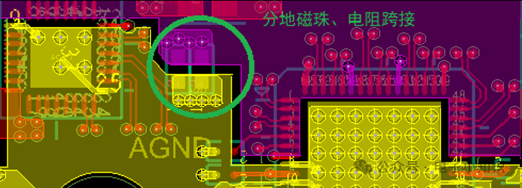
The common ground bridge does not provide a signal return path, only serves as an equipotential short circuit.
-
For multiple ADCs, it is best to have one pair share a common bridge.
-
Analog Area Plane Treatment
-
All layers in the analog area must be completely isolated, and all layers in the analog area should be grounded.
-
Digital signal wiring is prohibited from entering this area.
-
Power supply for the analog area should use signal layers for copper or traces.
Old rule: Old friends like, new friends follow, continuously share PCB practical skills, and enhance the value of technical personnel!
 Form a theoretical knowledge discussion group! Note: Discussion group!