Shenzhen Jinhanyu Electronics Co., Ltd
Luhua CJC6811A
A USB digital audio chip based on Cortex core


Overview
Description
The CJC6811A is a USB digital audio chip based on the Cortex core.
It integrates a 32-bit RISC CPU and 16KB SRAM, USB, UART, IIC, audio codec, GPIO, TIMER, WDT, PWM, SPI, IIS, SARADC, PLL, LDO, etc.
The CJC6811A boots from the internal FLASH via the SPI interface. After power-up, the firmware is read from the internal FLASH memory into the internal SRAM for execution.
The CJC6811A can operate at up to 48MHz to minimize power consumption while allowing flexibility for high performance.
It includes clock gating for individual IPs, and the CJC6811A can operate in different power-saving modes: normal, idle, standby, and power-off, with different clock and power strategies for each mode.
PART 01.
Performance Features
Cortex core
LDO
Built-in LDO, operating voltage range: 3.3V
Memory
Supports up to 16KB of program memory
RAM: 16KB SRAM memory: 16KB SRAM
ISP and ICP online programming via USB/SPI bus
Clock Control
Programmable system clock source
4-6MHz built-in RC oscillator (1% accuracy at 25℃)
12MHz clock from USB oscillator
Supports external crystal oscillator
10kHz internal low-power DC oscillator for watchdog and idle wake-up
USB Compatibility
Compatible with USB 1.0/1.1/2.0 low-speed/full-speed modes
Compatible with USB Audio 1.0 protocol
Compatible with USB Human Interface Device protocol 1.1
Supports USB suspend/resume/reset functions
Supports control, interrupt, bulk, and synchronous data transfer
Audio Codec
Default sampling rates: 192kHz / 176.4kHz / 96kHz / 88.2kHz / 48kHz / 44.1kHz
Supports bit lengths: 16/20/24/32bit
DAC supports up to 192kHz/16bit, ADC supports up to 48K/16bit
I/O Ports
4 General I/O (GPIO)
Timers
3 internal timers
Selectable internal or external clock source
Can generate interrupts on overflow and timeout
Each timer has two match registers
Supports incrementing and decrementing modes
Watchdog Timer
Outputs one or more signals during timeout
—– System reset
—– System interrupt
—– External interrupt
32-bit down counter
Selectable internal or external clock source
Reset timeout period is variable
Access protection
PWM
One 16-bit timer PWM channel
Programmable duty cycle control for output waveform
Automatic reload mode or one-shot pulse mode
Capture and compare functions
UART
Programmable baud rate, up to 921.6K
SPI
A designated SPI interface, as an AHB device for the bootloader and an APB device for write-back
Speeds up to 40MHz
I2C
Compatible with Philips IIC standard
I2S
Supports I2S format
Supports master/slave mode and 16/24-bit data width
SARADC
1 analog input
8-bit SARADC, 7-bit precision guaranteed
Power-off Reset
Programmable 3 threshold values: 2.7V/2.4V/2.0V (default 2.0V)
Optional BOD interrupt or reset
Operating Temperature: -40~+85℃
Storage Temperature: -55~+125℃
Package Type: QFN5*5-32
Moisture Sensitivity Level: MSL3
PART 02.
Important Diagram References

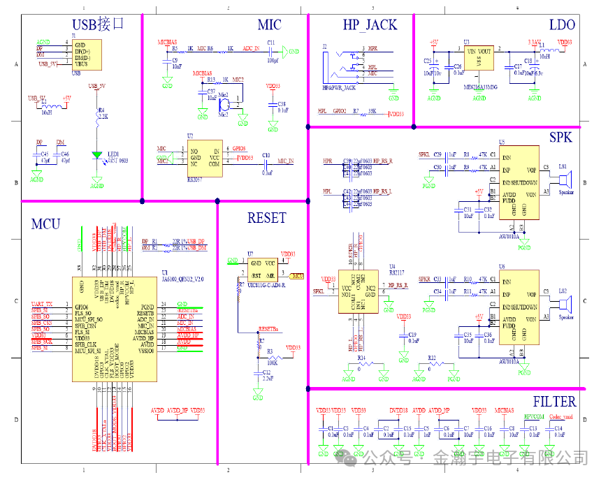
Reference Design Schematic


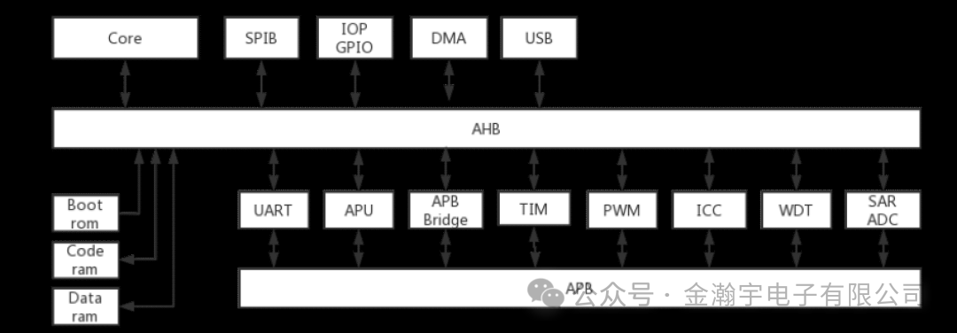
Chip Block Diagram


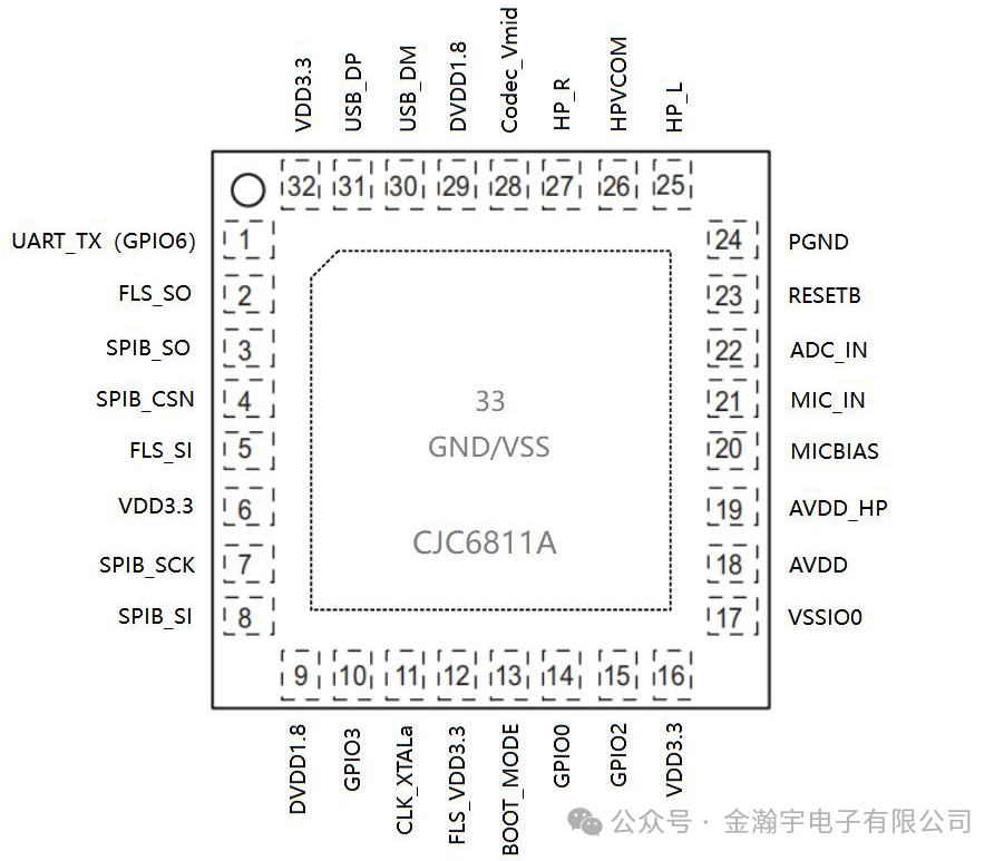
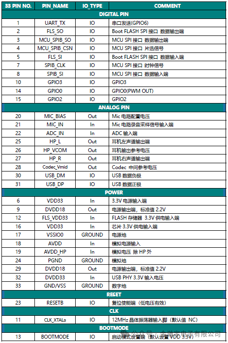
Package and Pin Definition

PART 03.
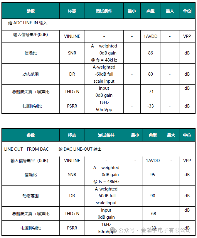
Electrical Characteristics
Test conditions: AVDD = AVDD_HP = VDD33 = VCCA2 = VCCA1 = VDD_IO1 = 3.3V, all modules powered on, TA = 25℃ (unless otherwise specified)
PART 04.
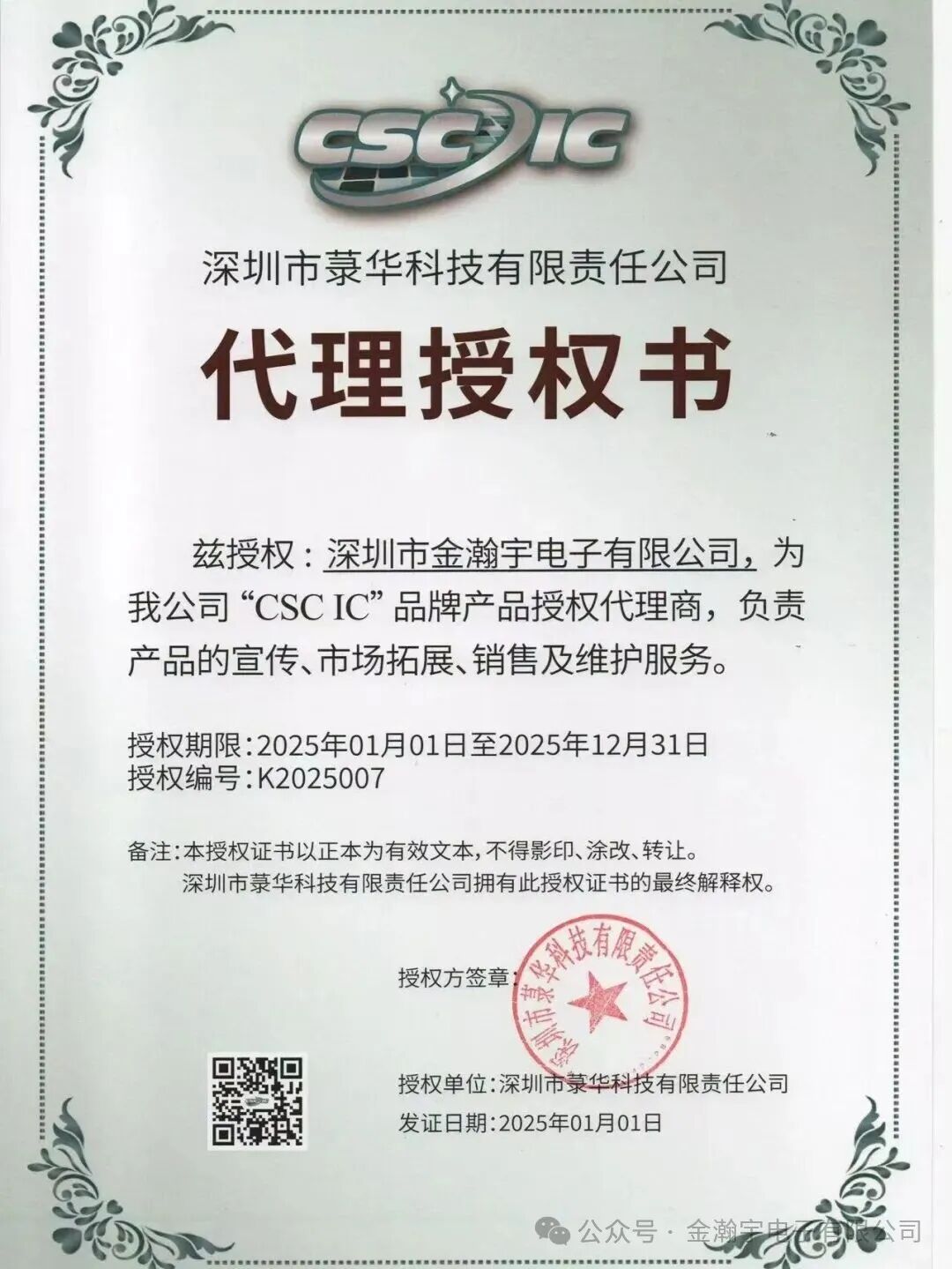
Agency Authorization

-END-

>> Reply with the model number to obtain the relevant data sheet
Looking forward to cooperating with you!