This project is a real project practical training, focusing on low-power UPF design. The backend parameters are as follows:
Process: 12nm
Frequency:2.5GHz
Resources: 2000_0000 instances
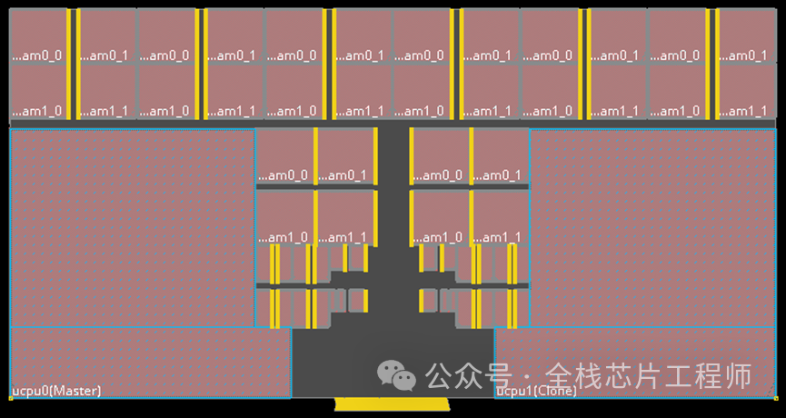
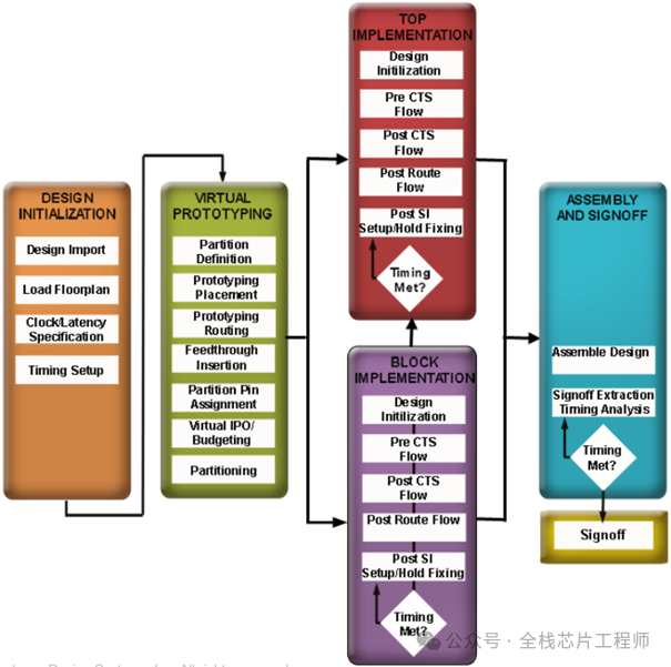
Flow: Partition Flow
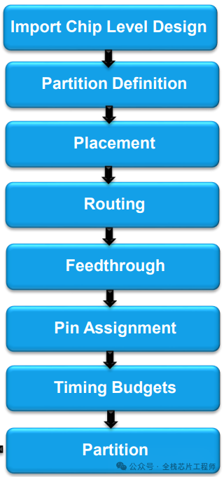
Partition Steps:
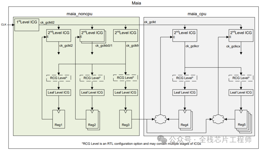
Clock Structure Analysis:
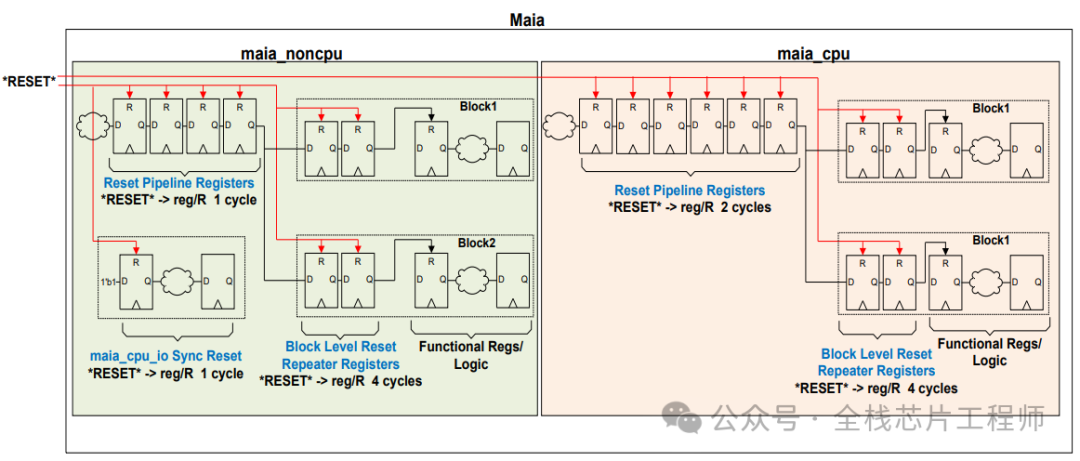
Reset Structure Analysis:
Cortex-A7 single core:
Gates=240291 Cells=118421
Cortex-A72 single core:
Gates=3125649 Cells=1207766
28nm Cortex-A7 single core:
12nm Cortex-A72 single core:
Area=486100.9 um^2
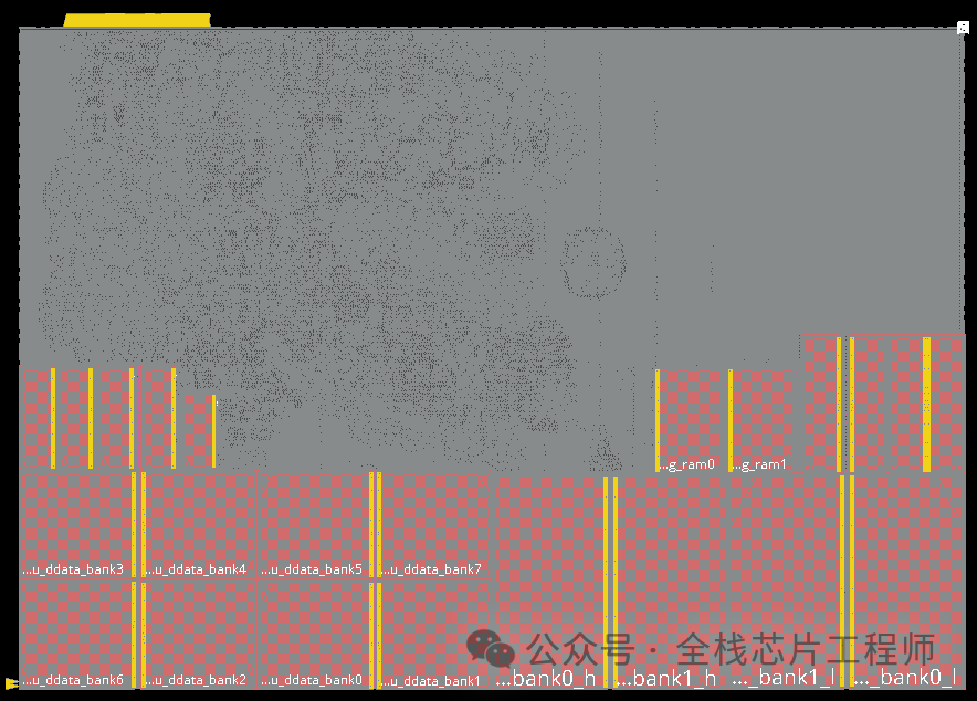
Cortex-A72 Processor Partition Flow:
Cortex-A7 Processor:
SoC Full Process Design Service
Chip Training (Real Projects) Introduction:
-
The only nationwide low-power image SoC front-end, mid-end, and back-end full process practical training
-
DDR4/3 project practical training
-
ARM Cortex-A72 processor 12nm PR practical training
-
ARM Cortex-A72 processor 12nm DFT practical training
-
Cross-clock domain RTL design and CDC practical training
-
UPF design and low-power simulation practical training
Chip Design Service Introduction:
-
Providing SoC, MCU, ISP, CIS and other chip design, verification,DFT design services
-
Providing DDR/PCIE/MIPI/CAN/USB/ETH/QSPI/UART/I2C IP design
-
Providing back-end design for 7nm, 12nm, 28nm, 40nm, 55nm, 65nm, 90nm
-
Providing customized chip design services and design training for universities and enterprises
【Enable every student to design an SoC/MCU chip】
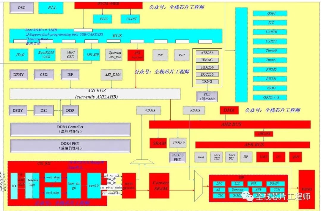
【The only one on the internet】Jingxin SoC is a low-power ISP image processing SoC used for 【chip full process design training】, featuring a low-power RISC-V processor, built-in ITCM SRAM, DTCM SRAM, and integrated IPs including MIPI, ISP, USB, QSPI, UART, I2C, GPIO, Ethernet MAC controller, designed using SMIC40 process.
-
High-speed interface Verilog design implementation -
From image algorithms to RTL design implementation -
MIPI, ISP Verilog implementation and simulation -
Lint, CDC checks andUVM verification -
Post-simulation
The content of just the front-end course is equivalent to 5-6 courses from other training institutions.
-
DFT design (chip-level) -
Synthesis logic synthesis (chip-level) -
Low-power UPF design, CLP technology -
Formal verification and other technologies
(3) In the SoC Back-end Course, you will learn:
-
Low-power design
-
Layout and wiring (low-power FF flow) -
StarRC/QRC -
STA/Tempus -
Power analysis -
DRC/LVS design
The content of just the back-end course is equivalent to 3-4 courses from other training institutions.
Join the knowledge community and become part of the chip design knowledge repository!
The Knowledge Community of SoC Training Camp