
The global demand for semiconductors and chips has surged in recent years, but the industry also faces multiple challenges such as software-defined transformation, explosive growth in AI computing power, sustainability, and global supply chain diversity.
“Software-defined vehicles, including software-defined devices, are becoming a trend. The CEO of the renowned automotive manufacturer Mercedes-Benz stated that the company is transforming into a software company, which says it all.” Ling Lin, Global Vice President of Siemens EDA and General Manager of Siemens China, delivered a speech titled “Are We Ready?—Reconstructing the World with AI, Defining the Future with Software” at the ICCAD 2025 conference, where his opening remarks precisely outlined the profound changes the semiconductor industry is undergoing.
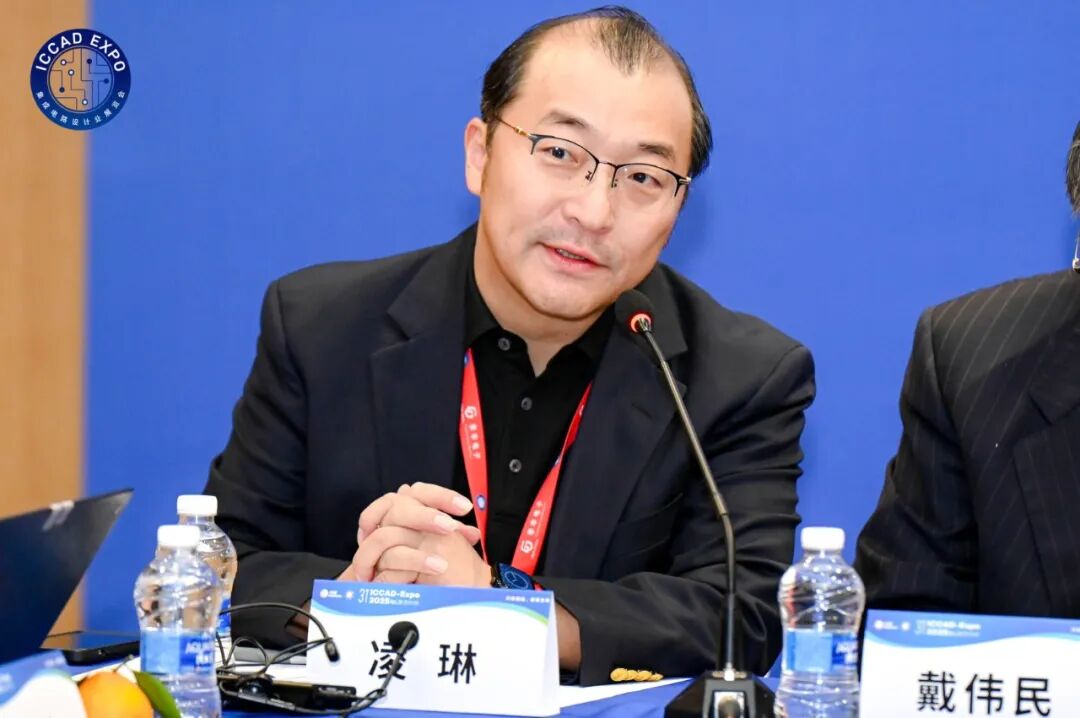
Ling Lin, Global Vice President of Siemens EDA and General Manager of Siemens China
Ling Lin pointed out that the semiconductor industry is facing three major real challenges: explosive demand, soaring costs, and declining success rates. The explosive growth of generative AI (with an adoption rate exceeding 60%), the wave of software-defined vehicles, the demand for sustainability (the electricity consumption of AI in the U.S. is expected to rise from 2% to over 12% in ten years), and the fragility of the global semiconductor supply chain. At the same time, the industry is also encountering severe real dilemmas—”75% of projects face delivery delays, the success rate of first-time chip tape-outs continues to decline, while R&D costs are soaring—$90 million for 16/14nm, $250 million for 7nm, and nearly $540 million for 3nm.”
“With 2022 as a watershed, the growth rate of global chip demand is astonishing.” Ling Lin emphasized in his speech that the semiconductor industry is transitioning from “strong demand” to “accelerated demand,” with the market size expected to exceed $1 trillion by 2030 (IBS estimates it will reach $1.2 trillion), and the acceleration from $1 trillion to $2 trillion will bring not just simple “involution,” but systemic challenges. New methodologies, tools, and collaborative approaches are needed to solve these structural problems.
How can EDA achieve comprehensive digital twins from chip-level to system-level?
“The semiconductor industry was one of the first to realize digital twins, due to its complex processes and large scale. Without suitable digital twin tools, it is impossible to define, design, and produce a chip.” Ling Lin pointed out that as Moore’s Law slows down and process complexity increases, the semiconductor industry is entering a new era of explosive growth in design complexity, and the EDA industry essentially supports the digital twin of the semiconductor industry.
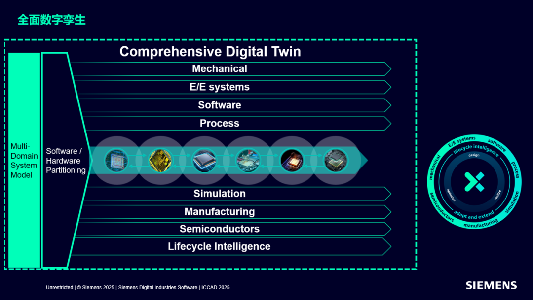
He proposed that the three pillars to solve industry challenges are “software-defined, chip-enabled, and AI-empowered,” and these three support “comprehensive digital twins”—from chip-level to system-level closed-loop verification.
“Comprehensive digital twins are not just an accurate mapping of the digital environment to the physical environment, but also encompass chips, PCBs, systems, as well as mechanical and subsystem electrical and electronic systems, even including software layer maintenance. This has elevated the concept and definition requirements of digital twins to a higher level, necessitating a more complete closed-loop digital twin to ensure that the projects and products produced can guarantee quality and be successfully launched,” Ling Lin said.
In China, Siemens EDA has implemented this concept. Ling Lin shared a case in collaboration with SAIC’s Chip Engineering Center, where its PAVE360 platform built a virtual software system for SAIC’s Chip Engineering Center, enabling software definition, system verification, power consumption assessment, and even road-level simulation in the cloud before the chip is taped out and hardware is in place.
“We have shifted ‘in-vehicle testing’ to the ‘design phase,’ making chip, subsystem, vehicle performance, metrics, and power consumption all clear at a glance, greatly improving R&D efficiency and compressing development cycles.” Ling Lin said. This “shift left” thinking is the core of “software-defined”—allowing the virtual world to lead, reducing physical trial and error..
AI Empowering EDA: From Theory to Industrial Application
“In recent years, AI has been talked about too much, but done too little.” Ling Lin emphasized in an interview that AI will not completely replace engineers, but will take over repetitive tasks, allowing engineers to focus on more innovative work. Today, AI has become the core foundation of Siemens EDA’s technology layout, with the company’s AI strategy focusing on “industrial-grade, mass-producible, accurate AI model applications.”
It is reported that Siemens has established a strong AI R&D system: with over 1,500 engineers dedicated to AI R&D, accumulating 3,700 AI patents over the past decade. “Siemens EDA leverages Siemens’ strong R&D capabilities and patents, using AI functions as a foundation to support EDA tools and processes,” Ling Lin mentioned in his speech: “We launched the foundation of our AI strategy at the DAC conference in June in the U.S.—the EDA AI System, which is a cross-product AI platform that combines NVIDIA NIM with Siemens’ own AI database to form a unified AI capability center.”
In terms of specific applications, Siemens EDA has integrated AI into its flagship products:
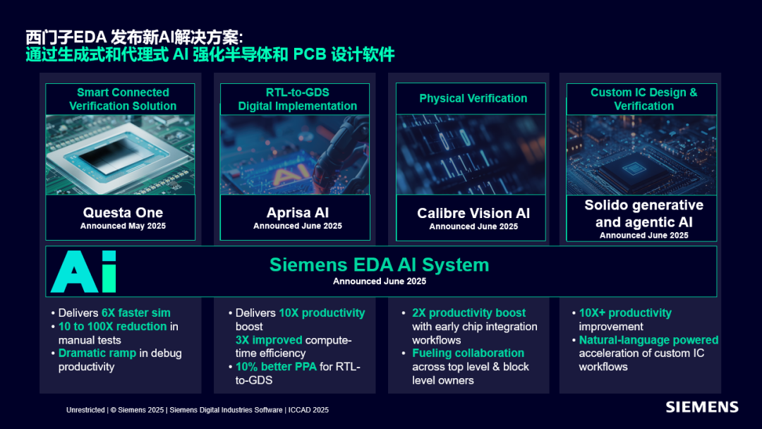
·Calibre Vision AI: Automatically identifies design violations, accelerates the chip assembly process, and addresses issues when “the chip size is large and time-consuming, requiring significant computing power”;
·Aprisa AI: Used for layout and routing;
·Questa One: Accelerates RTL-level verification, significantly improving simulation efficiency;
·After acquiring Solido Solutions in 2017, AI technology was expanded from a single product to the entire toolchain, achieving an order of magnitude speedup in simulation, and by 2018, AI was already applied to the toolset, expanding from one product to various other products.
In the face of industry skepticism regarding “AI black boxes” and “data silos,” Ling Lin believes that AI is not a “panacea,” but an “industrial-grade foundation,” and its application in EDA must be “verifiable, mass-producible, and explainable.” He revealed that Siemens EDA adopts a “progressive embedding” strategy, from data layer, algorithm layer to tool layer, allowing AI to grow within the tools, enabling customers to benefit without feeling it.
Today, Siemens EDA has launched AI-powered tools, where all data used is based on past experience accumulation, including publicly available customer data being integrated together, applying AI algorithms and patents to support each toolset. “Ling Lin emphasized that this is a gradual process, and Siemens EDA’s AI applications focus on “verifiability, usability, universality, accuracy, and stability,” ensuring they meet industrial-grade mass production requirements.
Chiplet and 3D IC: Building a Complete Ecosystem
With the exponential increase in R&D and tape-out costs, the semiconductor industry is increasingly aware that it can no longer rely solely on advanced processes. 3D IC, Chiplet, and heterogeneous integration have become hot topics in chip design in the post-Moore era, and Siemens EDA is promoting a complete closed loop from “design to verification to production” for 3D IC.
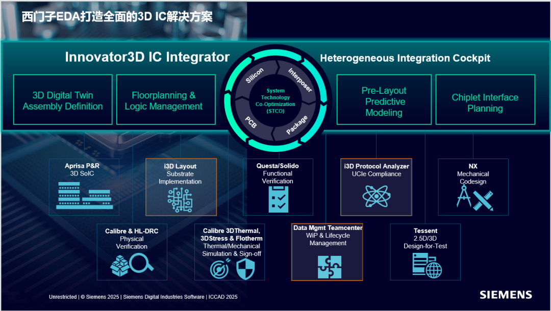
“In June of this year, we launched the Innovator3DIC Integrator, which is like the ‘cockpit’ for 3D IC development, providing overall planning and management functions. This suite includes Innovator3D IC Layout, Innovator3D IC Layout Protocol Analyzer, and Innovator3D IC Data Management, which address physical design, signal integrity simulation, and version management challenges. Additionally, Siemens EDA has also released Calibre 3DThermal and Calibre 3DStress tools for thermal stress and stress analysis of high-density 3D ICs.
Ling Lin pointed out: “These tools can perform multi-physical field simulations to ensure design reliability.”
Siemens EDA has also joined the OIP 3DFabric alliance established by TSMC, “certifying all important EDA tools within the alliance for everyone to use as soon as possible.” At the same time, Siemens EDA has collaborated with Intel to validate all tools, meaning that the company’s customers can freely utilize these suites to quickly deploy 3D IC design, verification, and manufacturing.
However, Chiplet is not simply about stacking blocks; it involves system-level, multi-physical field, and cross-process collaborative design. Ling Lin emphasized that Siemens EDA’s Innovator3D IC platform not only provides design tools but also integrates “thermal, stress, signal integrity, and power integrity” for joint simulation capabilities across multiple physical fields.
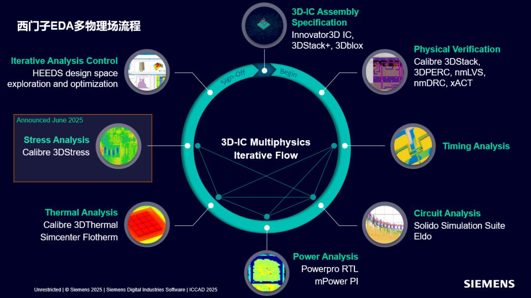
Thermal issues should not only be considered during the packaging stage but should be addressed by extracting thermal models during the design phase. “On Calibre, we have also added 3D thermal analysis and stress analysis models to our flagship products, enabling customers to have a smooth process from design to verification to production, truly achieving closed-loop design.” Ling Lin said. This capability is particularly crucial for the Chinese industry, as when advanced processes are limited, Chiplet + 3D IC represents a new pathway for Chinese chips to break through.
Recent Developments at Siemens EDA
Public information shows that Siemens is continuously enriching its industrial software ecosystem through a series of acquisitions and collaborations:
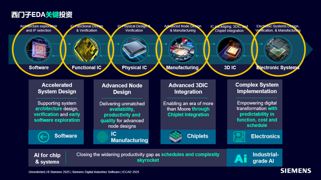
·Acquisition of Excellicon: Enhances timing constraint management capabilities;
·Acquisition of Downstream: Expands PCB production data preparation capabilities, connecting with mainstream CAM350 suites;
·$10.6 billion acquisition of Altair: Altair has strong capabilities in HPC, AI data analysis, and electronic-mechanical simulation integration, enabling Siemens to perform more comprehensive cross-physical domain simulation work;
·$5 billion acquisition of Dotmatics: Accelerates the physical R&D process in pharmaceuticals, expanding the boundaries of industrial software applications;
In terms of strategic cooperation, Siemens EDA has established deep partnerships with Alphawave Semi (high-speed interface IP), Perforce (IP lifecycle management tools), and Arm (Neoverse collaboration).
“Siemens industrial software is always looking for ways to enrich its ‘arsenal’ while building an ecosystem, categorizing and completing industrial software.” Ling Lin stated, “We cannot do everything ourselves, but we can integrate the best technologies into our platform to help customers solve problems in a one-stop manner.”
It is reported that Siemens EDA has already established partnerships with over 80 universities in China and has been promoting the “Assistant Engineer” program since 2007, training hundreds of industry backbone talents.
Building a Healthy Ecosystem to Meet Future Challenges
Ling Lin repeatedly emphasized the core viewpoint in his speech and interviews: “Integrating the physical world with the digital world is actually the main purpose and task of comprehensive digital twins.” He pointed out that the future trend of EDA development is “software-defined, chip-enabled, and AI-empowered,” and that “comprehensive digital twins can truly ensure that every point is well done, breaking through demand across the entire value chain, rather than engaging in mutual involution and profit squeezing within a single chip or subsystem.”
In terms of ecosystem construction, Ling Lin called for: “Strengthening collaboration among upstream and downstream in the industry, as well as with ecological partners. Only then can we solve more difficult problems and issues of involution, because relying solely on localized optimization of the supply chain cannot yield actual value; only global optimization can create a value chain, allowing everyone in the industry to focus on their own tasks, which is the healthiest ecosystem.”
“Are you ready? We are ready, are you ready?” Ling Lin’s closing question in his speech is not only a call to the industry but also a commitment from Siemens EDA—to use the most comprehensive digital twin platform and solutions to help customers tackle the most challenging technological evolutions and the most complex product design and mass production challenges. As he stated, “Reconstructing the world with AI, defining the future with software.”

THE END
Follow “Electronic Engineering Magazine” and add the editor’s WeChat
Regional groups are now open, please send messages 【Shenzhen】【Shanghai】【Beijing】【Chengdu】【Xi’an】 to the public account