SWD: Serial Wire Debug

SWD (Serial Wire Debug) is one of the two debugging ports currently supported by ARM (the other being the JTAG Debug Port). SWD reads and writes the chip’s registers by transmitting data packets, serving as a two-wire protocol for accessing the ARM debugging interface, and is part of the ARM Debug Interface Architecture Specification, often regarded as a replacement for JTAG. Here is a detailed analysis of SWD:
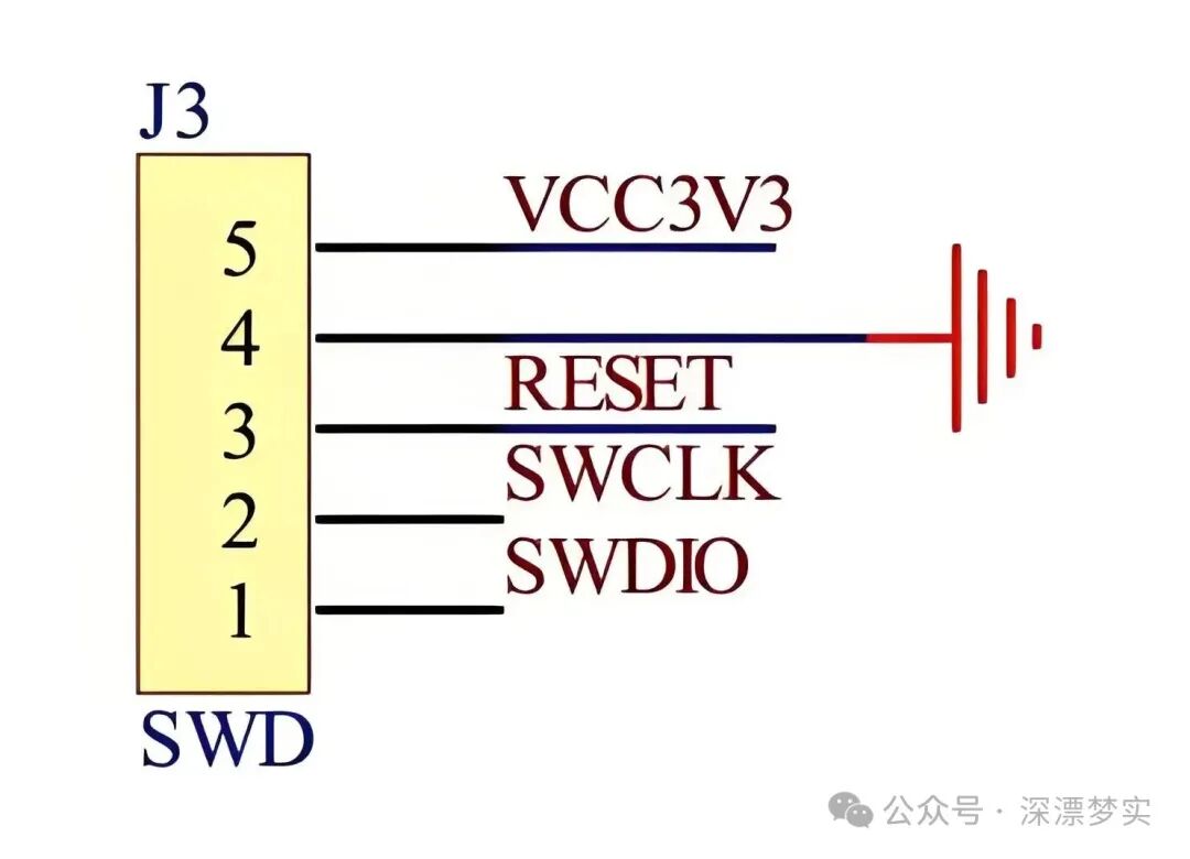
1. Interface Composition
The physical layer of the SWD interface consists of two lines:
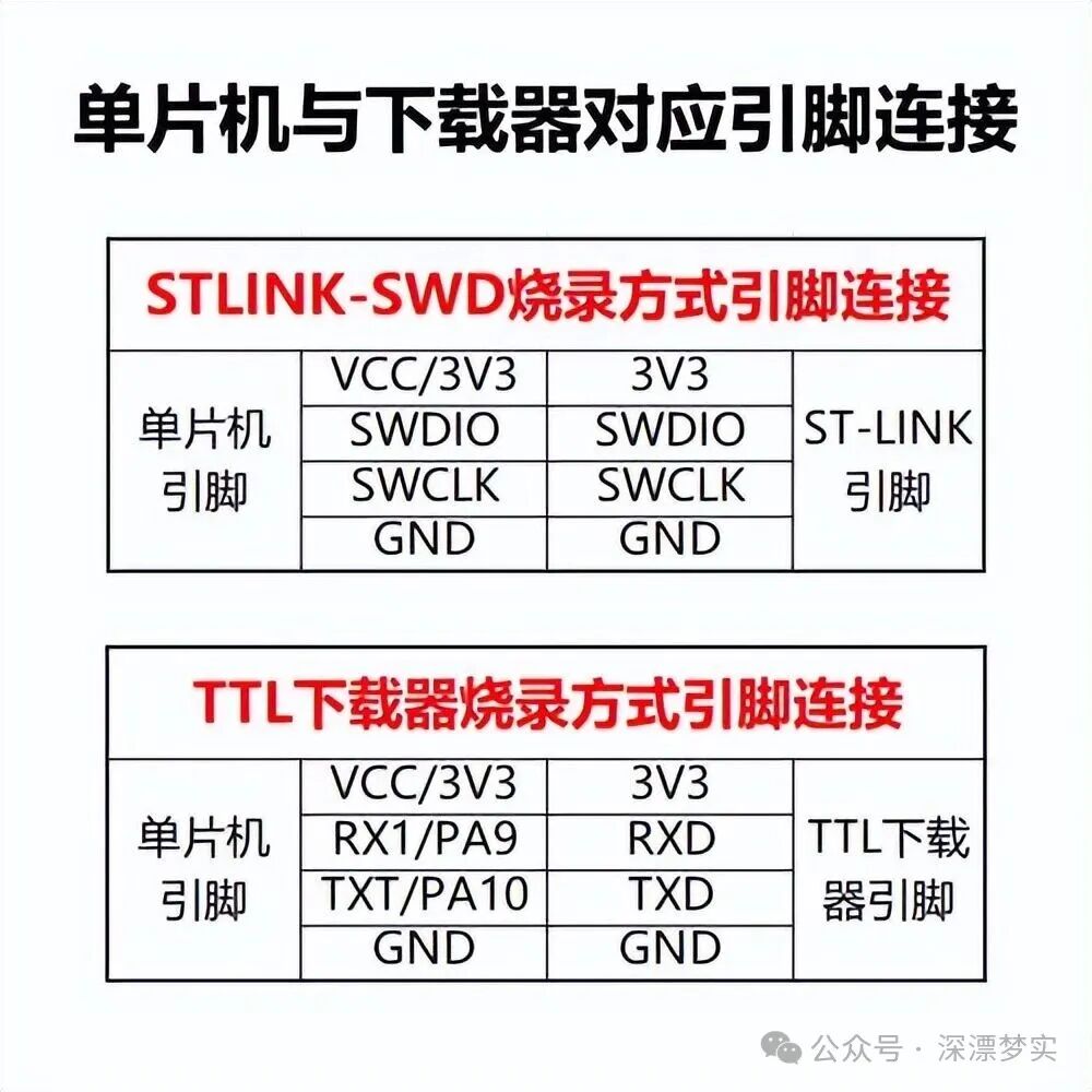
SWDIO: Bidirectional data line used for transmitting data and instructions.
SWCLK: Clock line driven by the host, used for synchronizing data transmission.
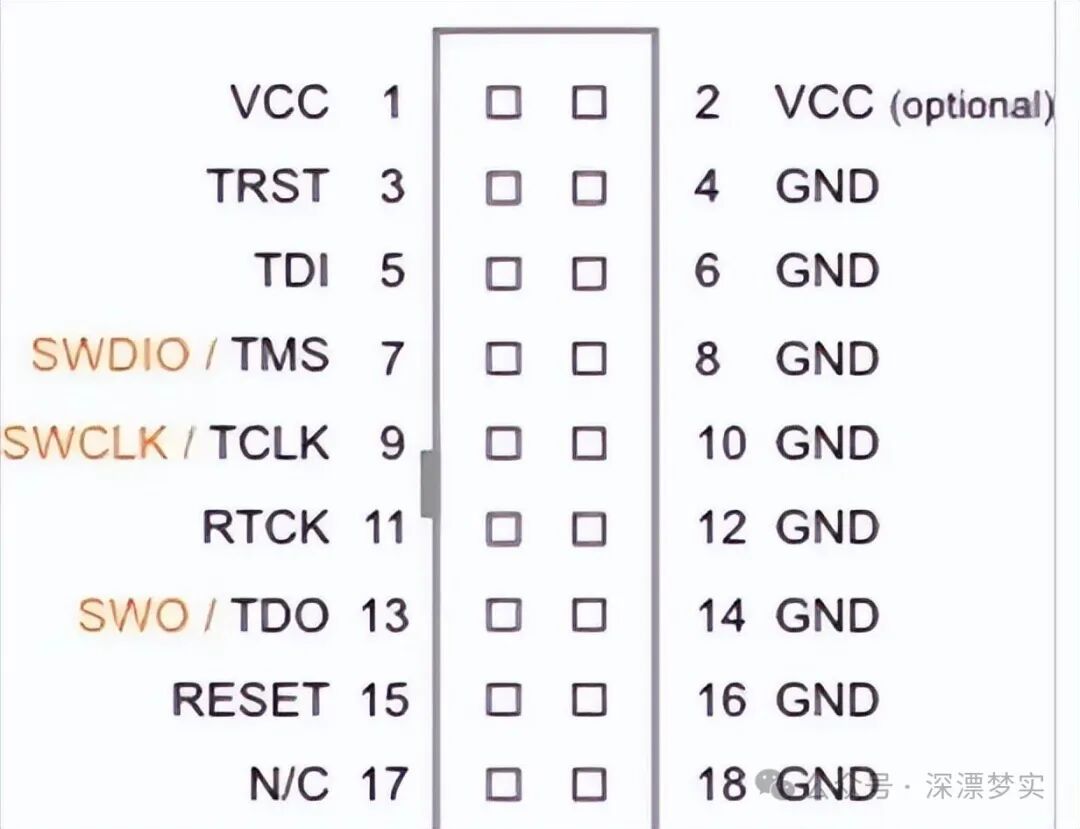
2. Working Principle
SWD transmits data through the SWDIO and SWCLK lines. The clock signal is input from the SWCLK pin, while the data signal is input/output from the SWDIO pin. The entire SWD operation process is hierarchical; first, the debugger operates on the SW-DP (Serial Wire Debug Port) to determine the parameters of the AP (Access Port) registers, and then operates on the Cortex Memory Map.
The control of the lines during the data phase depends on the type of request issued by the host. If the host issues a write request, it will drive the SWDIO line; during a read request, the target will drive the SWDIO line to transfer data from the target to the host. In all phases, data is transmitted starting with the LSB (Least Significant Bit). Whether the target samples data from the SWDIO line or drives data onto the SWDIO line, it occurs on the rising edge of the SWCLK clock.
3. Main Features
1. Simplified Hardware:
The SWD interface requires only two lines, significantly simplifying hardware design compared to the multiple pins of JTAG, making it easier to integrate into resource-constrained systems.
2. High-Speed Communication:
SWD uses a serial communication method, reducing communication overhead and is generally faster than JTAG.
3. Low Power Consumption:
Due to the fewer pins and efficient communication method, SWD typically has lower power consumption.
4. Built-in Reset Protocol:
The SWD interface usually comes with a built-in reset protocol, eliminating the need for an additional RST reset pin.
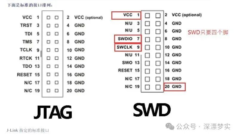
4. Application Examples
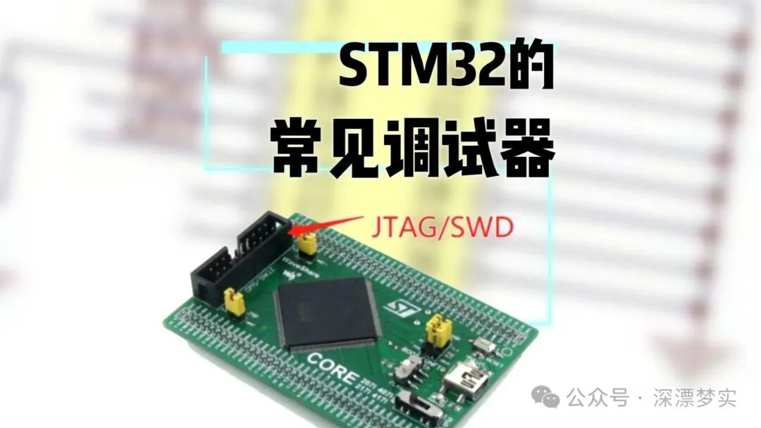
The SWD interface is widely used in debugging ARM Cortex-M series microcontrollers, such as the STM32 series chips. These chips typically integrate the SWJ-DP (Serial/JTAG Debug Interface), which includes both JTAG-DP and SW-DP interfaces. During debugging, the debugger (such as ST-link or J-link) connects to the SWDIO and SWCLK pins to perform debugging operations on the microcontroller.
5. Precautions
1. When using the SWD interface for debugging, ensure that the connection between the debugger and the target device is correct.
2. Before performing debugging operations, some configuration or initialization may be required, such as setting the debugging mode, reading the IDCODE, etc.
3. Due to the relative simplicity of the SWD interface, it may not provide as rich functionality as JTAG in debugging complex systems. When choosing a debugging interface, comprehensive consideration should be given based on project requirements and hardware support.
In summary, SWD, as an efficient and low-cost debugging interface, plays an important role in embedded system development and debugging. With the widespread application of ARM Cortex-M series microcontrollers, the SWD interface will also see broader promotion and application in the future.
FollowWeChat Official Account: Deep Dream Reality for more valuable content sharing!