
Click the Blue Text
Follow Us
1. What is SPI
SPI stands for Serial Peripheral Interface, which is a serial interface for peripheral devices. SPI is a high-speed, full-duplex, synchronous communication bus with a master-slave structure, occupying only four lines on the chip pins, saving pin space and providing convenience for PCB layout. Due to these simple and user-friendly characteristics, more and more chips are integrating this communication protocol.
2. Application Scope
The SPI protocol mainly serves as the interface protocol for the master control chip to configure peripheral chips. The SPI interface is primarily used between EEPROM, FLASH, real-time clocks, AD converters, digital signal processors, and digital signal decoders.
It occupies only four lines on the chip pins, saving pin space and providing convenience for PCB layout. This simple and user-friendly feature has led to an increasing number of chips integrating this communication protocol.
PCB (Printed Circuit Board)
3. Protocol Features
SPI is a high-speed, full-duplex, synchronous communication bus. It is important to note that SPI only distinguishes between master and slave modes, without the concept of read and write, as each SPI communication involves data exchange between the master and slave devices. In other words, sending data will always result in receiving data; to receive data, one must first send data.
1) Transmission Rate
The transmission rate of the SPI bus needs to be defined by the user, with no specific regulations, generally ranging from 400KHz to 10MHz.
2) Main Functions
To connect the MCU with various external devices (chip-to-chip connections) and to exchange data in a serial manner (serial-parallel conversion).
3) Topology Structure
A single SPI Master can connect multiple SPI Slaves through shared data lines (one master, multiple slaves);
4) Interface Configuration
As an interconnection interface between chips, it configures the peripheral chip (SPI Slave) through the control chip (SPI Master) using configuration registers;
4. SPI Bus Principle
SPI is a ring bus structure that follows a master-slave configuration, suitable for scenarios with one master and multiple slaves. SPI communication requires four lines: three bus lines and one chip select line, as shown in the physical connection below:
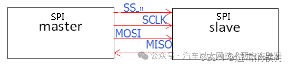
The timing is quite simple, primarily involving data exchange between two bidirectional shift registers under the control of SCLK.
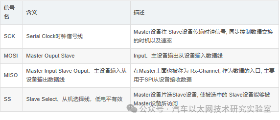
5. Signal List
SS, SCK, and MOSI signals are generated by the master device, while the MISO signal is generated by the slave device. The MOSI and MISO signals are only valid when SS is low, transmitting one bit of data during each clock cycle.
6. SPI Transmission Timing
During communication, a data link loop occurs between the Master and Slave devices.
There are four different data transmission timings for SPI, depending on the combination of clock polarity (CPOL) and clock phase (CPHA).
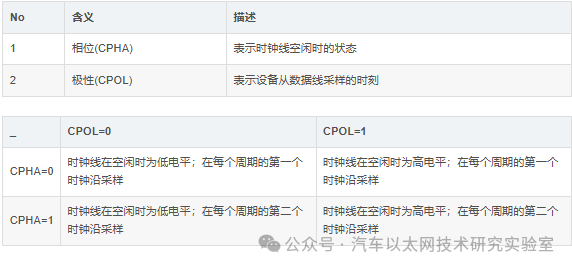
1) Mode 0
CPOL= 0, CPHA=0. The SCK serial clock line is low when idle, data is sampled on the rising edge of the SCK clock, and data switches on the falling edge of the SCK clock.
2) Mode 1
CPOL= 0, CPHA=1. The SCK serial clock line is low when idle, data is sampled on the falling edge of the SCK clock, and data switches on the rising edge of the SCK clock.
3) Mode 2
CPOL= 1, CPHA=0. The SCK serial clock line is high when idle, data is sampled on the falling edge of the SCK clock, and data switches on the rising edge of the SCK clock.
4) Mode 3
CPOL= 1, CPHA=1. The SCK serial clock line is high when idle, data is sampled on the rising edge of the SCK clock, and data switches on the falling edge of the SCK clock.
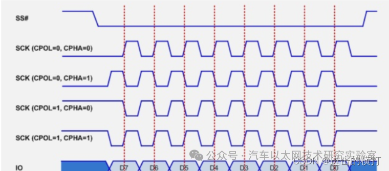
The commonly used modes are Mode 0 and Mode 3. To clearly describe the timing of the SPI bus, the SPI timing diagram under Mode 0 is shown below:
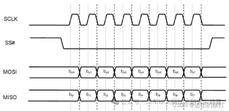
The above diagram clearly indicates that under Mode 0, in the idle state, the SCK serial clock line is low. When SS is pulled low by the master, data transmission begins, and the data switching (Toggling) of MOSI and MISO occurs on the falling edge of the clock (the black dashed line in the diagram), while the data sampling of MOSI and MISO occurs in the middle of the data (the gray solid line in the diagram).
7. Data Exchange
The data transfer between SPI devices is referred to as data exchange because the SPI protocol stipulates that an SPI device cannot act solely as a “Transmitter” or “Receiver” during data communication. In each Clock cycle, SPI devices send and receive a bit of data, equivalent to exchanging a bit of data.
A Slave device must be accessed by the Master device beforehand to receive control signals sent by the Master. Therefore, the Master device must first select the Slave device using the SS/CS pin to access the desired Slave device.
During data transmission, each received data must be sampled before the next data transfer. If previously received data is not read, it may be discarded, resulting in the failure of the SPI physical module. Therefore, in the program, it is common to read the data from the SPI device after the SPI transmission completes, even if this data (Dummy Data) is useless in our program.


*Disclaimer: This article is originally written or forwarded by the author. If any party’s intellectual property rights are inadvertently infringed, please inform us for deletion. The above images and text are sourced from the internet. If there is any infringement, please contact us in a timely manner, and we will delete it within 24 hours. The content of the article reflects the author’s personal views, and the Automotive Ethernet Technology Research Laboratory reproduces it solely to convey a different perspective, which does not represent the Automotive Ethernet Technology Research Laboratory’s endorsement or support of this view. If there are any objections, please contact the Automotive Ethernet Technology Research Laboratory.
Original Link:
https://blog.csdn.net/Last_Impression/article/details/140067418