Source: Semika
Original Author: Semika
Introduces common semiconductor-related terms used in the manufacturing, design, testing, and packaging processes.
TAPEOUT (TO):Tape Out, refers to submitting the final GDSII file to the foundry for processing.
FULL MASK:Full Mask, means that all masks in the manufacturing process serve a specific design.
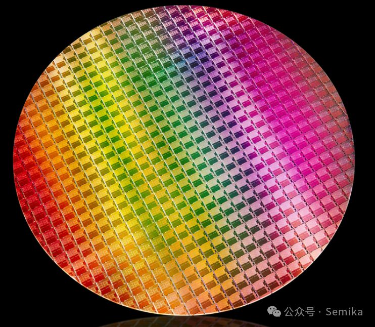
MPW (Multi Project Wafer):Multi Project Wafer, means that multiple projects share a single wafer, allowing multiple IC designs to be manufactured in the same process.
MPW shares a mask with other manufacturers, while FULL MASK has a dedicated mask. If the chip risk is high, MPW can be done first, and if testing is fine, then FULL MASK can be done.
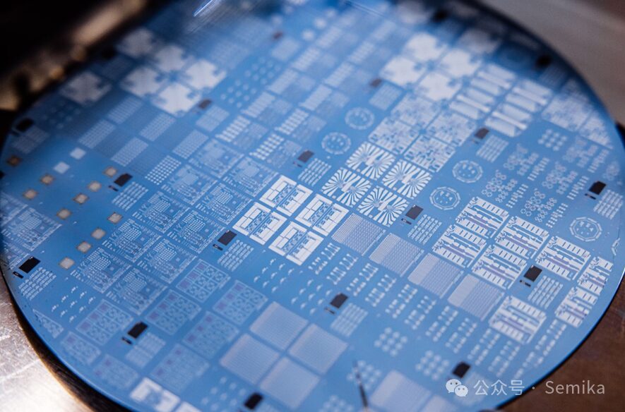
Foundry:Wafer Fab, is a manufacturer specializing in chip manufacturing, corresponding to fabless, which is a design manufacturer without a wafer fab.
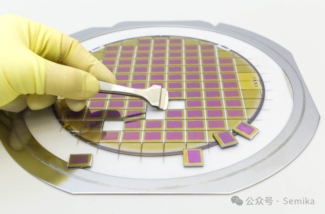
Die:After wafer cutting, a single chip’s wafer, which needs to be encased to become a chip.
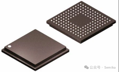
Chip:The final encapsulated chip.
Bump:Protrusion, bumps on the wafer surface (gold, tin-lead, lead-free, etc.), often used in flip chip packaging.
Mask: A mask is an opaque graphic template covering selected areas on the silicon wafer, which allows only the areas outside the selected region to be affected by subsequent etching or diffusion.
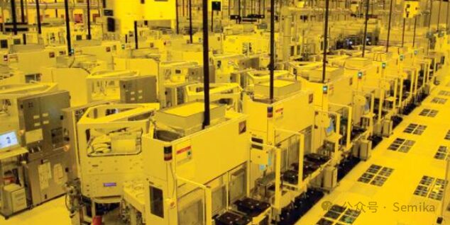
Chamber: Vacuum chamber/reaction chamber, specifically refers to a sealed space with special purposes such as vacuum extraction, gas reactions, or metal sputtering.
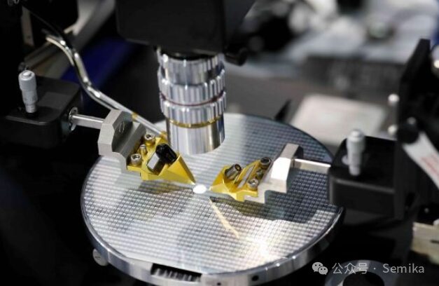
Dicing Wafer:Wafer dicing, wafer cutting.
CVD (Chemical Vapor Deposition):Chemical vapor deposition, is an advanced technology widely used in material preparation, converting chemical substances in gases or gas mixtures into solid materials under high temperature and low pressure conditions.
PVD (Physical Vapor Deposition):Physical vapor deposition, is a method of attaching another material to a substrate surface using ion plasma technology. It is a collective term for spraying, evaporation, etc.
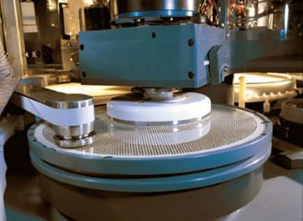
CMP (Chemical-Mechanical Polish):Chemical-mechanical polishing, uses polishing pads filled with abrasive particles to flatten uneven crystal surfaces through a combination of chemical reactions and mechanical grinding.
CDA (Clean Dry Air):Compressed dry air, typically refers to air with a pressure between 60 to 110 psi, which has been purified and dried. It serves as a gas source for pneumatic components.
Diffusion:In the semiconductor industry, diffusion is often performed on very pure silicon chips using preset or ion implantation methods to create a diffusion source, completed within hours at high temperatures in a furnace.
DI Water:Deionized water, tap water or groundwater contains a large number of bacteria, metal ions, and particles, which must be sterilized, filtered, and purified using equipment, and then the metal ions and other impurities are removed; the resulting water is called “deionized water” and is specifically used for IC manufacturing.
Dopant:Doping, refers to the active implantation or diffusion of other atoms or ions into the original semiconductor material to change its electrical properties.
Dummy Wafer:Dummy wafer, a silicon wafer that assists in the process and differs from the product. Generally, the quality requirements for it are not very high.
Fabless: is a combination of Fabrication (manufacturing) and less (none), referring to an operational model of integrated circuit design that focuses solely on design without manufacturing capabilities, often used to describe IC design companies that do not own chip manufacturing facilities.
RTL (Register-Transfer Level): A hardware description language used to describe synchronous digital circuits.
SDC (Synopsys Design Chip): Provides constraint files for design; synthesis tools require this constraint file to convert RTL into netlist. The main content of SDC includes: chip operating frequency, chip IO timing, design rules, special paths, and paths not to be checked, etc.
Verification: Chip functional verification, mainly refers to the methodology of verifying whether the RTL and reference model are consistent.
Simulation: Simulation, typically generates waveforms; generally, chip functionality, verification, and chip power consumption can be simulated, providing an intuitive reflection of real scenarios.
IP (Intellectual Property): Design assets, functional circuit modules (cores, units) that have been designed and verified.
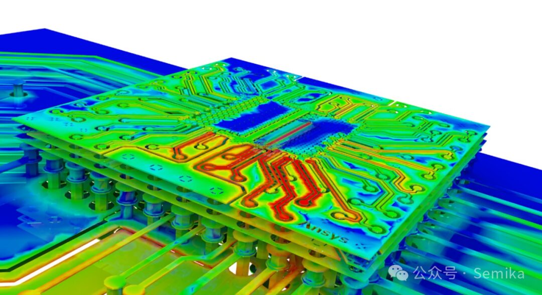
Design Rule: Design specifications, because semiconductor process technology is a specialized, delicate, and complex technology, it is easily influenced by different manufacturing equipment and process methods (RECIPE). Therefore, when considering how various products can be manufactured successfully, a set of specifications must be established to regulate the relevant technical aspects, known as “Design Rule”, which is formulated according to various product needs, specifications, manufacturing equipment, process methods, process capabilities, and relevant electrical parameter specifications.
CP (Chip Probing): Directly tests the wafer, targeting each Die on the entire wafer to ensure that each Die meets the device characteristics or design specifications, usually including voltage, current, timing, and functionality validation.
FT (Final Test): The final interception before the chip leaves the factory. The target of testing is the packaged chip; after CP testing, it will undergo packaging, followed by FT testing. This can be used to detect the process level of the packaging factory.
CP targets the wafer; if a Die is faulty, there is no need to package it, saving packaging and substrate costs. After CP testing, chip failures may still occur during packaging, so FT is also needed to eliminate defective chips.
Yield: Yield, the yield of chips is related to the process; there is a certain probability of chip failure, and the larger the chip, the greater the failure probability.
IP (Intellectual Property): Refers to complete functional modules of integrated circuits that are verified, reusable, and possess specific functionalities in integrated circuit design. IP can be classified into License and Royalty based on charging methods. IP is the most essential component of chips; for example, USB, PCIe, CPU, etc., are all IPs. The entire chip is an integration of IP, allowing for complex chip functionalities, primarily through IP reuse. For example, those with tens of millions or billions of gates can only be achieved through IP reuse.
DUV (Deep Ultraviolet Rays): Deep ultraviolet rays.
EUV (Extreme Ultraviolet Rays): Extreme ultraviolet rays.
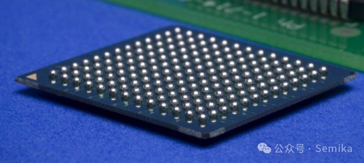
BGA (Ball Grid Array): A type of surface mount packaging, where multiple solder balls are set on the chip mounting substrate (ball grid array).
ASIC (Application Specific Integrated Circuit): Application-specific integrated circuit, ASIC is a special chip designed specifically for a certain requirement. For example, dedicated audio and video processors, and many dedicated AI chips can currently be considered a type of ASIC.
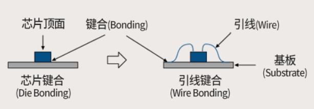
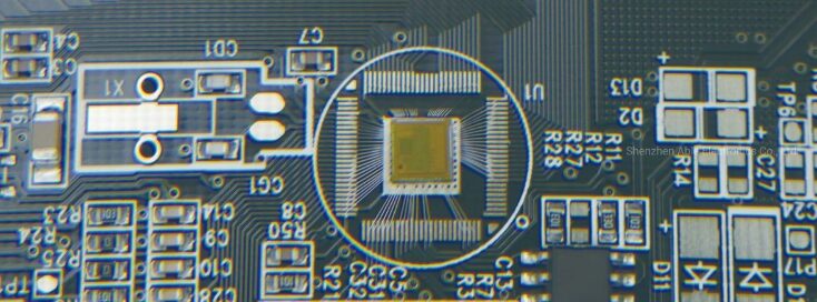
Wirebonding: Wire bonding, also known as wire bonding (pressure welding, also called bonding, connection, or wire welding), refers to using metal wires (gold wire, aluminum wire, etc.) to connect the internal wiring of solid-state circuits, i.e., the connection between the chip and the circuit or lead frame, using thermal pressure or ultrasonic energy.
Flipchip: Flip chip, where solder balls are deposited on the I/O pad, and the chip is flipped over and heated to combine the molten solder balls with the ceramic substrate.
COB (Chip-On-Board): Chip-on-board packaging, where bare chips are attached to the PCB using conductive or non-conductive adhesive, and then wire bonded to achieve electrical connections, with glue encapsulating the chip and bonding wires.
SOC (System On Chip): System on a chip, which integrates the CPU, bus, peripherals, etc., into a single chip. For example, a mobile phone processor is a complex SOC chip.
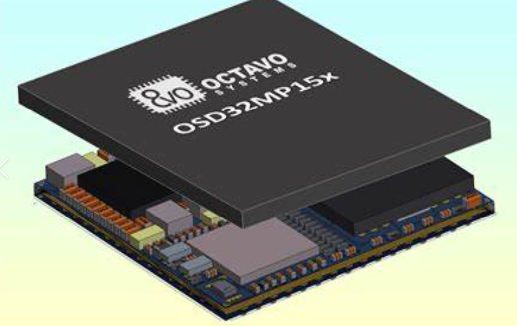
SIP (System In Package): System-in-package, SiP packaging integrates different functional bare chips, including CPU, GPU, memory, etc., into a single package, forming an entire chip system.
SOP (Small Outline Package): A type of small outline package where the leads are pulled in two directions.
DAF (Die Attach Film): Die bonding film bonding process.
CMOS (Complementary Metal Oxide Semiconductor): Complementary metal-oxide-semiconductor. It refers to a technology used to manufacture large-scale integrated circuit chips or chips made using this technology, which is a writable RAM chip on the computer motherboard. Due to its writable characteristics, it is used on the computer motherboard to store BIOS settings after setting the computer hardware parameters; this chip is only used for data storage.
END
Reproduced content only represents the author’s views
Does not represent the position of the Institute of Semiconductors, Chinese Academy of Sciences
Editor: March
Editor: Six Dollar Fish
Submission Email: [email protected]
1. The Semiconductor Institute has made progress in research on bionic covering neuron models and learning methods.
2. The Semiconductor Institute has made significant progress in inverted structure perovskite solar cells.
3. Why is copper used as the interconnect metal in chips?
4. What exactly is 7nm in chips?
5. Silicon-based integrated optical quantum chip technology.
6. How abnormal is the quantum anomalous Hall effect? It may lead to the next revolution in information technology!