1. What is Tape-Out
Tape-out, in English, refers to the process of converting the layout of a designed integrated circuit (IC) into an actual chip, similar to a production line, through a series of manufacturing steps.
Tape-out, which means sending for manufacturing, is the final stage of integrated circuit design, where the chip design company (Fabless) submits the completed design to a foundry for the production of a batch of sample chips (usually ranging from dozens to hundreds), to verify whether each manufacturing step is feasible and whether the circuit meets the required performance and functionality.
2. Why is Tape-Out Necessary?
Tape-out is a prerequisite for mass production and serves as the ultimate test to verify the basic performance of the chip!
Generally, during the first tape-out, all layers need to be processed sequentially. Therefore, to test whether the integrated circuit design is successful, tape-out must be performed, transitioning from a circuit diagram to a chip, verifying the feasibility of each manufacturing step and checking whether the circuit possesses the desired performance and functionality. This process typically lasts at least three months (including material preparation, photolithography, doping, electroplating, packaging, and testing), and generally involves over 1000 manufacturing steps, making it the most critical and costly phase in chip manufacturing.
If successful, large-scale chip production can commence; otherwise, the reasons must be identified, and corresponding design optimizations made.
3. Why is Tape-Out So Expensive?
The process from chip design to finished product involves several key stages: Design -> Tape-Out -> Packaging -> Testing, with the BOM cost composition generally being 20% labor cost, 40% tape-out, 35% packaging, and 5% testing. Clearly, tape-out represents the largest cost component!
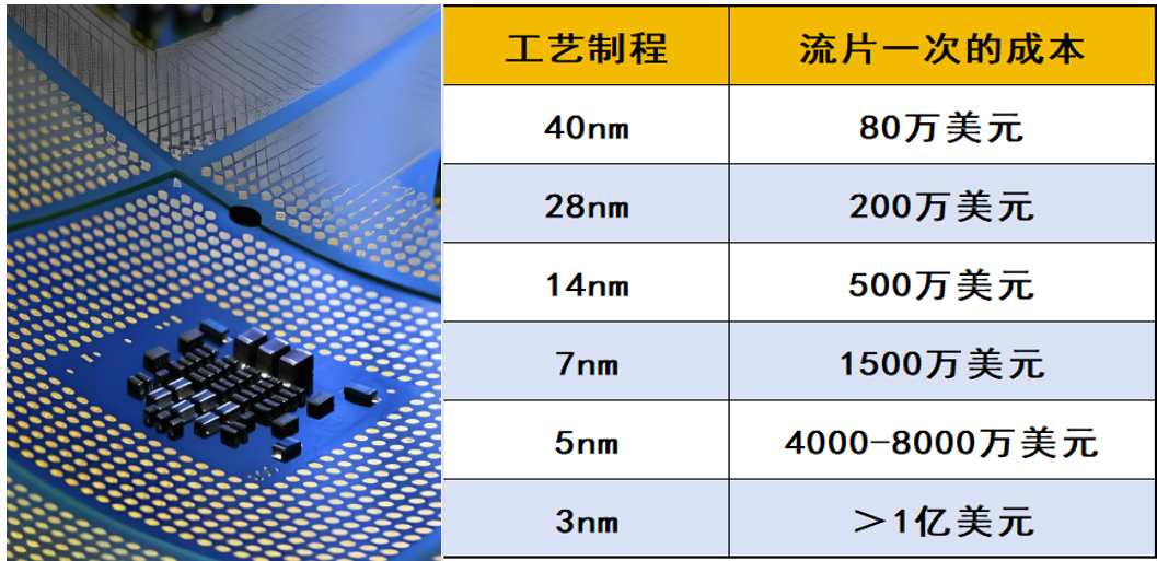
With the advancement of semiconductor processes, the costs of tape-out have been increasing exponentially. The cost of a single tape-out, depending on the process technology, is approximately as shown in the figure below:
The high cost of tape-out can be attributed to three main factors:
Firstly, the primary costs are associated with masks and wafers, both of which are expensive consumables. Among these, masks are the most costly, with a set of mid-range process masks costing around $500,000, while a single wafer can cost several thousand dollars.
Masks are akin to photographic negatives, and wafer processing involves copying the chip design layout (including shapes, sizes, layers, etc.) onto a semiconductor silicon wafer, similar to the imaging and developing process of a film camera.
Masks serve as the carriers of the original patterns during the photolithography process, where exposure and development transfer these pattern details onto the wafer. Thus, the quality of the mask directly determines the quality of the photolithography.
Since chip circuits are multi-layered and three-dimensional, with different shapes for each layer, chip manufacturing requires dozens of photolithography steps, necessitating a mask for each step. Each layer of the mask requires a coating of photoresist, followed by pre-baking, exposure, baking, and development processes.
28nm technology requires approximately 40 layers of masks, 14nm requires about 60 layers, and 7nm technology may require 80 layers or even over a hundred. Reports indicate that TSMC’s 5nm full mask tape-out costs around 300 million RMB.
As shown in the figure below, the application of masks in tape-out:
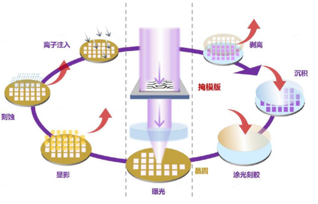 Secondly, the entire tape-out process involves hundreds of steps, including photolithography, etching, deposition, doping, etc. Each step requires highly precise control, leading to high operational costs.
Thirdly, tape-out is actually a form of non-mass production, characterized by small batch production, lacking the economic effects of large-scale production. Mass production can reduce costs through bulk material procurement and automated production lines, but these advantages are difficult to achieve in the tape-out model.
A chip development project undergoes a lengthy process from product definition, design, verification, and simulation to final tape-out, and as the “ultimate test,” any small oversight in the preceding lengthy process can lead to tape-out failure (the risk rate for chip tape-out is as high as 15%-35%). Once tape-out fails, it often means the company faces losses starting from tens of millions of dollars and a missed market opportunity of at least six months.
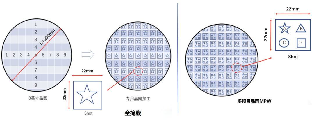
4. Methods of Chip Tape-Out (Full Mask, MPW)
Full Mask and MPW are both methods of tape-out for integrated circuits. Full Mask refers to “full mask”; while MPW stands for Multi Project Wafer, literally meaning multiple project wafers.
1) Full Mask, or “full mask,” means that all masks in the manufacturing process serve a specific design; a Full Mask chip can produce thousands of dies from a single wafer; then packaged into chips, it can support large-scale customer demand.
2) MPW, or Multi Project Wafer, is similar to panel prototyping in PCB design. Multi Project Wafer involves placing multiple integrated circuit designs that use the same process on the same wafer for tape-out. After manufacturing, each design can obtain several sample chips, which is sufficient for experiments and testing during the prototype design phase. This approach can reduce tape-out costs by 90%-95%, significantly lowering the cost of chip development.