The success rate of first silicon for chips is sharply declining due to the increasing complexity of chip manufacturing, the need for more iterations as manufacturers shift from single-chip to multi-chip components, and the growing demand for customization, which extends the design and verification process.
Details from a new functional verification survey highlight that developing advanced chips that are both functional and reliable is becoming increasingly difficult. In many cases, these devices are larger than photomask-sized systems on chip (SoCs) and contain various components and wiring schemes that may reduce their stability. Therefore, they require more optimization and more iterations.These devices integrate more logic circuits, some of which are developed on different process nodes. They have more static random access memory (SRAM) and more interconnect structures, both of which are developing at a different pace than logic circuits. Additionally, they require more software, as the development speed of software, particularly for large language models (LLMs) and other AI algorithms, is much faster than that of hardware. They also need complex thermal management technologies, new materials, carefully designed and customized packaging, and more precise workload-based models. Worse still, the verification time required is exceeding the scheduled timelines.
The cumulative impact of all these factors is reflected in the latest data. Harry Foster, Chief Verification Scientist at Siemens EDA, stated, “The industry is at a historical low point in achieving first silicon success. Historically, this rate has been around 30%. Two years ago, from 2023 to 2024, this rate dropped from 30% to 24%. Now it has fallen to 14%. This is one data point. Another data point is that historically, about two-thirds of projects are delayed. Now that rate has risen to 75%.”
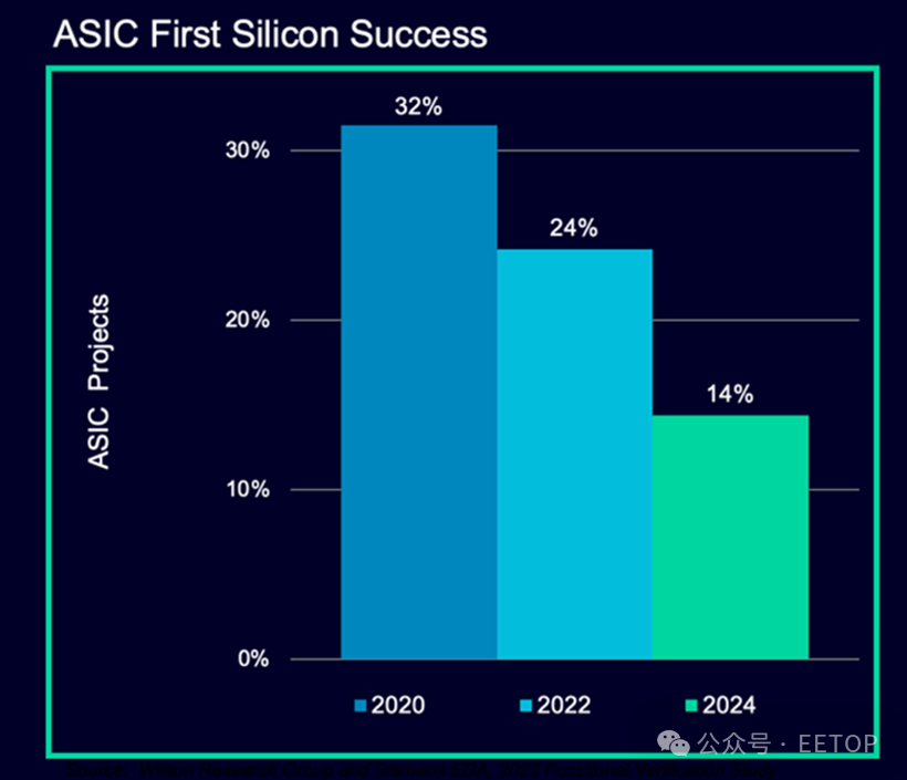
Figure 1: The number of designs that are functionally correct and manufacturable is declining.
Every step in the increasingly complex and multi-layered process requires improved production efficiency. Typically, this means hiring more engineers. However, due to a persistent talent shortage and the extensive training required far exceeding the knowledge base engineers previously needed, this is not feasible. This is why EDA vendors are so focused on integrating AI into their tools, essentially encoding this knowledge through reinforcement learning. But this transition still takes time.
Foster said, “What we are currently doing is not working. We need to significantly improve production efficiency, and this is not a metric many like to discuss because it is hard to measure. It is relatively easy to say, ‘this is 10% faster than that.’ Moreover, many companies lack the skills to design very complex chips, or this is new territory for them. In the late 1990s, everyone was talking about the production efficiency gap. The issues now are different from 20 years ago, but there are some common themes. We need to move from isolated toolsets to more interconnected and integrated tools.”
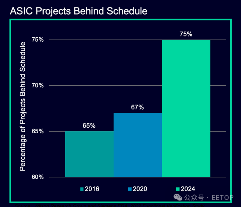
Figure 2: Increasing complexity, coupled with the production efficiency gap, is extending chip manufacturing times.
Source: Siemens EDA / Wilson Research / Design Verification Conference (DVCon)
However, the production efficiency issue cannot be entirely blamed on complexity. Even mainstream chip manufacturers are now producing chips faster than in the past.
Matt Graham, Senior Director of Verification Software at Cadence, stated, “I initially worked in verification, and we all seem to have some level of concern about first silicon success. For a long time, we seemed to be in that state. But in the past year to 18 months, suddenly everyone is producing more chips. Even those companies not focused on the consumer market, like those making chips for test equipment, are now seeing demand for chips that is four times what it used to be. They have gone from producing one chip every 18 months to producing 4 to 5 chips a year. This is because suddenly everything has become more specialized.”
Such situations often occur during significant technological shifts, where processes, tools, and standards need to catch up. Graham said, “We often move from specialization to generalization and then back to specialization, and we seem to be in one of those specific application cycles. This has increased the number of chips produced by everyone four to five times, but no one has increased staffing to handle the fourfold increase in chip tape-out work. And if you are at the cutting edge, adopting 3D integrated circuits (3D-IC) or chiplet-based designs, one wafer may require slight adjustments.”
In cutting-edge fields, changes are both profound and numerous, sometimes varying by design, making it difficult to pinpoint the issues. Many such designs are custom-tailored for large system vendors who wish to push performance limits for specific applications or data types. In these cases, the cost of re-taping is part of the budgeting process, which also introduces some uncertainty into the data.
Frank Schirrmeister, Executive Director of Strategic Projects and System Solutions at Synopsys, stated, “For re-taping situations, logical functionality remains the most prominent issue. The survey from [Siemens EDA / Wilson Research Group] shows that 70% of re-tapings are due to design errors caused by specification changes. This means someone misunderstood the specification requirements and sounded the alarm, leading to 50% of projects undergoing a second tape-out. Some large chip manufacturers actually expect to undergo up to four re-tapings. So ultimately, it still comes down to complexity.”
This also creates a significant potential opportunity for EDA companies, especially those incorporating some form of AI into their tools and processes.
Sassine Ghazi, CEO of Synopsys, stated during the Synopsys User Group keynote, “In generative AI, you have a ‘co-pilot’ to assist and create. With the ‘co-pilot’ technology we developed in collaboration with Microsoft, you have a workflow assistant, knowledge assistant, and debugging assistant. You can train junior engineers faster, and the same goes for senior engineers. They can interact with our products in a more modern, effective, and efficient way. Then there are the creative elements. We worked with customers early on to generate from register transfer level (RTL), test platform generation to test assertions, where you can have a ‘co-pilot’ to help you create parts of RTL, test platform documentation, and test assertions.”
In some cases, production efficiency has improved from several days in the past to just a few minutes now. But with the advent of agentic AI, the biggest benefits are still ahead, fundamentally raising the abstraction level of the entire design and verification process.
Ghazi said, “As AI continues to evolve, workflows will change accordingly. Our stakeholders often ask me when we will see changes in the EDA market through the use of AI. I believe that unless workflows change, meaning you can do certain things in a fundamentally different way to deliver products faster, more effectively, and more efficiently, this will not happen. Now, in the age of agentic AI, agent engineers will collaborate with human engineers to tackle complexity and change workflows.”
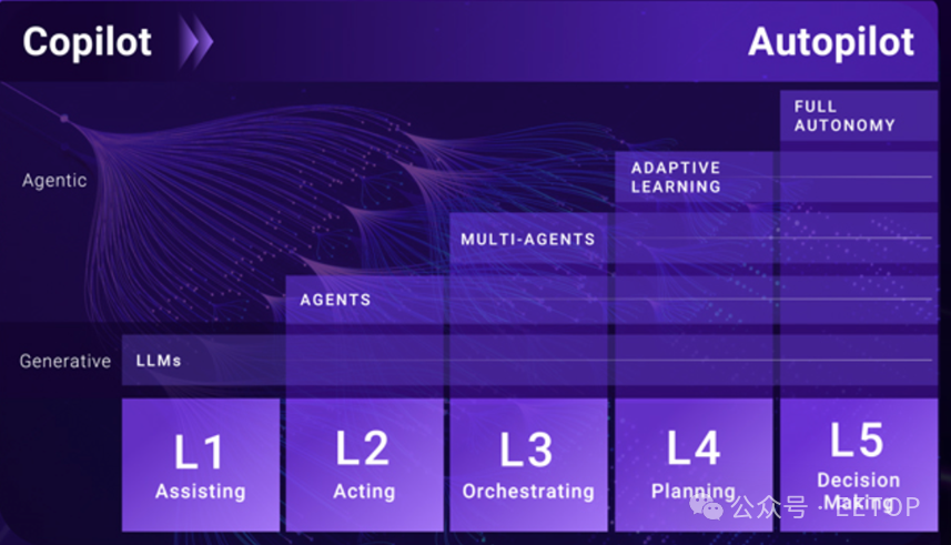
Figure 3: The evolution from generative AI to agentic AI. Source: Synopsys
Abstracting the Issues
One of the biggest challenges engineers face in advanced design is understanding the dependencies among hundreds or even thousands of different elements in the design. In the past, a key solution was to integrate hardware and software more closely. Today’s co-design may involve dozens or even hundreds of small chips that need to work independently and sometimes collaboratively. To understand all possible interactions, multi-physics simulations are required, and today’s co-design is no longer just hardware-software co-design; it also includes various types of interconnect structures, packaging, and possibly photonics, and in some cases even larger system-level systems.
Moreover, all designs need to be testable (design for testability, DFT), manufacturable (design for manufacturability, DFM), and have sufficient yield (design for yield, DFY), and they also need to have adequate internal controls to prevent overheating. If overheating does occur and aging happens faster than expected, there needs to be a mechanism for rerouting signals, which is primarily driven by software.
Graham from Cadence stated, “In the verification domain, we see software increasingly becoming part of the complete solution. It is no longer just ‘we want to make a chip.’ It is a specific chip. The end market and final application scenario for the chip are clear. The software stack running on the chip is known, and the robots, cars, or other devices that will embed the chip are also clear. And all these factors need to be considered from various angles; we need to think about software verification, pre-tape-out verification, and possibly even perfecting the software before putting it into a simulator or prototype platform.”
Initially, it is not always clear how much functionality software and hardware should each have. In complex designs, fine-tuning this balance is a time-consuming process that easily leads to multiple re-tapings.
Ashish Darbari, CEO of Axiomise, stated, “Software introduces a lot of functionality and features. If the hardware team, especially the verification team, is not fully aware of these, there will be a significant gap between what is being tested and what has been defined and scoped. This is why many bugs are missed. We do all this virtual prototyping and start the software early to get 10,000 or 100,000 simulation vectors. But who is looking at the boundary conditions? One project after another, we find all these error conditions in the first two or three weeks because the designers have run out of time.”
New Markets, Different Focuses
These issues extend far beyond functional verification and debugging, as functional verification and debugging have historically consumed the vast majority of chip development time and resources before manufacturing. The adoption of more complex chips in safety-critical applications such as automotive and military/aerospace has added entirely new requirements to designs. In the past, these markets did not allow the use of advanced node chips because they were considered unreliable. However, with increasing competition from electric vehicle startups like BYD and NIO in China, as well as Rivian and Lucid in the U.S., traditional automakers are racing to shift more functionality to software. This can only be achieved through the use of more advanced chips and highly customized packaging, and as automakers move towards higher levels of automation, this demand will become increasingly necessary.
In these systems, safety is a fundamental requirement, but any system failure can also lead to safety vulnerabilities. Therefore, chip designs need to consider more extreme conditions, from accelerated aging due to environmental heat in hot climates to real-world road conditions. While many of these situations can be simulated, chips also need to undergo road testing. If any issues cannot be adequately resolved through software, the chip will need to be re-taped.
Darbari from Axiomise stated, “Functional verification will consume most of your time. However, simple power optimization, such as introducing don’t-care values (X) in the design, can easily make a module susceptible to Trojan attacks because these don’t-care values now provide multiple choices in the execution framework. So in the chip, don’t-care values (X) are either 0 or 1. In reality, you won’t see don’t-care values (X), but from a simulation and behavioral perspective, these don’t-care values now add comprehensive choices for the end user, allowing them to operate in areas of the design that they should not have access to. So on one hand, you have functional verification. On the other hand, you have the power perspective introducing these don’t-care value issues, and then there are redundancy areas. In terms of security, the larger the area in the chip, the greater the exposure risk.”
Integrating the Parts
Chips require additional silicon area to accommodate more processing elements and more functionality, or to house multiple small chips in some advanced packaging. But this also makes achieving first silicon success more difficult.
Foster from Siemens stated, “You are dealing with accelerators that have very complex workloads. This introduces a lot of uncertainty in the design that we don’t even know how to semantically describe, making verification difficult. One of the challenges is that we have built many tool-centric processes without considering the feedback loops needed to optimize all of this. In the future, we need more interconnected processes. Only then can we leverage AI. A clear example is when I am doing design for testability (DFT), ‘oops, I can’t meet the fault coverage requirements.’ So now I need to manually go back to the early stages of the tool process. All these loops need to be closed. But where do we find people to do this work?”
According to EDA companies and some leading foundries and outsourced semiconductor assembly and test (OSAT) companies, the answer lies in new tools, methods, and possibly stricter design rules and more limited packaging options. But it is still too early to determine how all this will ultimately develop. The pace of change is much faster than anyone predicted a few years ago, and the data is proof of that.
*Disclaimer: This article is an original piece by the author ED SPERLING. The content reflects the author’s personal views, and the reprint by LuKe Verification is solely to convey a different perspective. If there are any objections, please feel free to contact LuKe Verification.