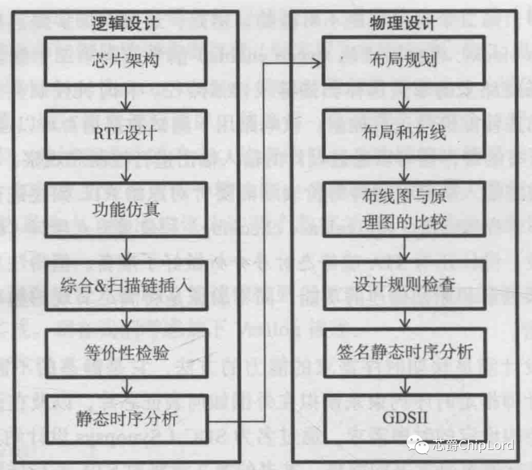
The typical ASIC design process can be divided into logical design and physical design.
Logical design starts with high-level design specifications and chip architecture. The chip architecture describes high-level functionality, power consumption, and timing (the speed at which the design operates) requirements. This is followed by a description of the design at the register transfer level, commonly referred to as RTL (register transfer level), which provides an abstract description of the circuit’s functional behavior based on how logical operations on signals allow data to flow between registers. RTL is typically described using hardware description languages (HDL) such as Verilog, System Verilog, or VHDL. After programming the functionality, verification is conducted through simulation. Simulation is a process in which various stimuli are applied to the design, capturing the design’s responses. The purpose of simulation is to verify whether the output matches the expected functionality of the circuit. For example, to verify an adder with two inputs and one output, test vectors provide the two numbers to be added as simulation inputs, and the output should be the sum of the two numbers. If the verification passes, the design is ready for synthesis.
Synthesis (also known as logic synthesis) is the step where the RTL description is transformed into a gate-level representation. The gate-level representation is an equivalent implementation of the functional hardware described using HDL.
For example, the following Verilog description:
module flipflop(d,clk,rst,q);input d,clk,rst;output q;reg q;always @(posedge clk)if(rst) q <= 1'b0; else q <= d;endmoduledefines a positive-edge triggered synchronous reset D flip-flop with three inputs and one output. When the clock has a positive edge, if the rst signal is 1, the output is 0; otherwise, the output is the value of d.
Synthesis tools can map the above RTL description to a positive-edge triggered synchronous reset flip-flop. If this HDL description can be mapped to a unique and unambiguous implementation using industry-standard synthesis tools, it is referred to as synthesizable RTL. During the synthesis step, designers also need to collect certain design and timing characteristics that represent the high-level goals outlined by the chip architecture, such as clock frequency, available delay of basic units, target libraries, etc., so that the synthesis tool can optimize the design to meet these requirements.
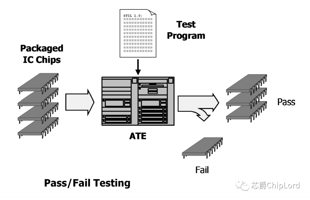
After synthesis is complete, the design begins preparations for DFT. DFT, or Design for Testability, refers to the insertion of various hardware logic during the chip design phase to enhance the chip’s testability (including controllability and observability). Through this logic, test vectors are generated to facilitate the testing of large-scale chips.
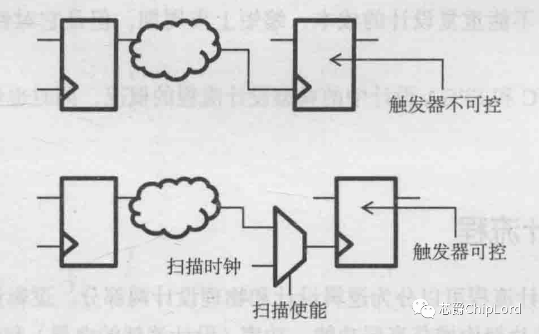
Consider the circuit in the figure below; the second flip-flop is uncontrollable. However, by adding a multiplexer (mux), the user can control the second flip-flop using the scan clock and scan enable signals. This method of linking all registers into a single chain is referred to as a scan chain or scan path. Similar to clock control, the data entering the flip-flop can also be controlled via the scan enable signal.
After synthesis and insertion of the scan chain, hardware equivalency representation needs to be verified against the original RTL to preserve design intent. This is known as equivalence checking and formal verification techniques. At this stage, the design is also prepared for STA or Static Timing Analysis. It is important to note that equivalence checking only verifies the functionality of the implemented gate-level representation against the original description, without checking if it meets frequency targets; verifying frequency targets is the responsibility of STA.
STA checks whether the design meets timing requirements; it is static and does not require simulation. Most STA engines require designers to specify timing constraints to simulate how the chip is characterized at the periphery and what assumptions are made internally to satisfy the timing requirements set by the chip architecture. The industry-standard format of SDC is used to make these specifications, completing the logical design step and serving as a bridge between logical design and physical design.
The physical design begins with layout planning. After preliminary timing analysis, the logical blocks of the design are laid out with optimization goals for area, aspect ratio, and communication between basic units. The goal is to ensure that there is not excessive internal switching, thus avoiding congestion and complications in routing. These factors directly affect power consumption, area, timing, and performance. Once the optimized layout planning is achieved, the connections between basic units begin to be routed.
During the synthesis phase, many assumptions are made about the clock network because hierarchical design information is not available until layout planning is completed. Following layout planning is clock tree synthesis, which aims to evenly distribute the clock to reduce clock skew between different parts of the design. Layout planning, placement, and routing steps are collectively referred to as design layout. In the physical design phase, as the assumptions made during the preliminary implementation phase become increasingly fixed, multiple STA executions may be required to complete a more accurate timing analysis.
At this stage, the IC layout needs to be verified to ensure compliance with the following conditions:
-
Compliance with all rules for manufacturing chips by the foundry, known as DRC, Design Rule Check;
-
Layout matches the netlist generated after synthesis, referred to as LVS, Layout Versus Schematic, which formally verifies the circuit layout against the final netlist.
Once the design has completed DRC and LVS, the sign-off for static timing analysis is complete. After layout, it cannot be guaranteed that the design meets timing requirements, and adjustments must be made to satisfy timing and frequency demands. Once the sign-off static timing analysis is complete, the design’s GDSII is generated. GDSII is a polygonal geometric representation that describes the actual layout of the design, including all connections; the fab factory produces chips based on the relevant GDSII.
The entire process from logical synthesis to physical design is referred to as the RTL2GDSII process, and the release of GDSII for chip production is known as Tapeout.
In summary, the ASIC design process is as follows:
Due to delays in viewing messages on the public account backend, please feel free to add WeChat for communication if there are any questions.