The complexity of ASICs is continuously increasing, and processes are constantly improving. Developing a stable and reusable ASIC chip design within a short time frame, and achieving a successful tape-out on the first attempt, requires a mature ASIC design methodology and development process. This article compares various ASIC design methods using EDA software such as NCverilog, DesignCompile, and Astro from the perspectives of process independence, system stability, and complexity. It introduces commonly overlooked issues and solutions during stages such as coding design, synthesis design, static timing analysis, and timing simulation, thereby enhancing the controllability of the entire design.
1. Basic ASIC Design Process
The ASIC design process can be roughly divided into front-end design and back-end design. For a more detailed division, it can be broken down into the following steps:
1. System architecture analysis design, RTL coding, and functional verification;
2. Logic synthesis, PreLayout STA, and formal verification (between RTL code and the netlist generated from logic synthesis);
3. Floorplan, Placement, Clock Tree insertion, and Global Routing;
4. Formal verification (between the netlist from logic synthesis and the netlist with CT information), STA;
5. Detailed Routing, DRC;
6. Post-layout STA, gate-level simulation with back-annotated delay information;
7. Tape-Out
Of course, this is still a relatively coarse process, where each step can be further divided. The so-called front-end design mainly includes steps 1, 2, 4, and 6 from the above process. Additionally, this process is iterative. Many common issues and methods have been extensively discussed in literature, so this article will focus on discussing some easily overlooked or potentially dangerous areas in each design stage.
2. Structural Analysis Design and RTL Coding
This stage plays a very important role in the entire ASIC design. The structural analysis design phase mainly starts from the functional definition of the product, performing a preliminary evaluation of the technology, power consumption, area, performance, and cost of the product, thereby formulating the corresponding design plan. For large-scale ASIC designs, estimating the chip’s power consumption and area at this stage can be very challenging.
Here, we introduce a very important concept in ASIC design: Partitioning. This concept will be mentioned in different design stages. First, functional partitioning must be done at the top-1 level of the chip. The top-1 level can usually be divided into four large functional modules: IOPads, boundary scan logic, core functional logic, and PLL clock module. Then, the core functional logic is further refined based on functionality. The core functional part will be the focus of RTL coding design, which will be elaborated upon below.
2.1 Good Coding Style
Coding style has a significant impact on the correctness, readability, maintainability, and performance and area of the synthesized chip. Naturally, it is impossible to elaborate on all issues encountered in coding in a single paper. Below, we will focus on some frequently encountered areas that may lead to errors.
From the perspective of reusable design and the consistency of code simulation behavior with actual chip behavior, it is necessary to adopt process-independent design. Some engineers may use delay elements or delay lines in coding to generate a pulse for operation. However, since delay elements are sensitive to temperature, voltage, and manufacturing processes, changes in these factors can also alter the width of the generated pulse. Therefore, there may be no issues during simulation or under certain operating conditions, but the actual chip may not work according to design goals when conditions change.
When coding at the RTL level, it is advisable to avoid instantiating standard cell gates, as this not only reduces code readability but also requires repeated modifications of the code when adopting a new cell library or new process. Synthesis tools will not perform logical optimization on these codes.
Other issues, such as potential latch problems caused by not assigning values to all condition branches, sensitivity list issues in always blocks, and the choice between blocking and non-blocking assignments, have been mentioned in many literatures, so they will not be repeated here. Below, we mention an easily overlooked issue: when defining timing blocks, some signals need to be reset, while others do not. If these are written in the same always block during coding, the synthesized circuit will not behave as we envisioned. For those signals that do not require resetting, the synthesizer may connect the reset signal to the enable terminal of the corresponding flip-flop, leading to inconsistencies between the RTL code and the netlist behavior. This type of problem cannot be detected during formal verification and may only be discovered through extensive gate-level simulation.
ASIC design should avoid using latches as timing elements. Potential issues with latch design include: if the enable input has a glitch, it may cause the latch to capture noisy data. Even if you can ensure that the data stable time can encompass the enable signal, it is difficult to guarantee that there are no glitches at the D input during the moment the enable is turned off, especially when receiving bus data. Meanwhile, latch design also brings difficulties for STA and DFT. By using flip-flops, potential issues can be reported through setup/hold time checks. Therefore, despite the advantages of latch design in terms of area and low power consumption, these potential risks make the design uncontrollable, so it is not recommended.
Try to avoid using clocks as signals. There may be no issues during RTL verification, but if these points are neglected in back-end design regarding clock skew control, unexpected results may occur. For example:
module gen_clk(cka,rst_n,ckb);
input cka,rst_n;
output ckb;
reg[1:0]ck_cnt;
always@(posedge cka)begin
if(!rst_n) ck_cnt
else ck_cnt
end
assign ckb=ck_cnt;
endmodule
This code will not have any issues during RTL simulation, while the potential problems will be discussed later.
2.2 Synchronous Design and Cross-Clock Domain Data Transfer
Although asynchronous systems have many advantages, such as low power consumption, they do not have the clock distribution and skew problems that trouble engineers in synchronous systems. However, their complex handshake protocols and difficulties in testing asynchronous circuits make synchronous systems still the first choice in digital circuit design. One characteristic of synchronous design is that all timing elements are sensitive to the same clock edge. It is unrealistic for the entire chip to use a single clock, so data transfer between asynchronous clock domains and some related issues will be the focus of this section.
Generally, to enable better synthesis and STA, it is necessary to partition the design. The general principle is to isolate parts that exchange data between asynchronous clock domains for separate processing, while other modules work within a single synchronous clock domain. How to handle these modules specially during the synthesis process will be discussed in the following sections. This section mainly discusses issues that need to be considered in code design.
The metastability problem between asynchronous clocks is mainly caused by the sampled data changing very close to the sampling clock edge, causing the output of the receiving (sampling) flip-flop to be metastable, which can lead to logical errors during transmission, commonly referred to as synchronization failure. This problem in synchronous clock domains is a hold problem, which can be eliminated using EDA tools or by inserting buffers, as EDA tools can detect such issues. In asynchronous receiving designs, two stages of flip-flops can be used to eliminate the possibility of metastability. There are now tools available to detect potential metastability issues in code. Issues caused by skew between multiple control signals, as shown in Figure 1, can occur if one bit, such as C2, has a delay greater than C1. The sampled data at Ck would appear as C2=1, C1=0, while it should be 00 according to the no-skew transmission waveform. Skew is unavoidable, possibly due to skew in the launch clock of signals C2 and C1, or due to transmission delays. For simple cases, we can simplify the logic to ensure that control signals are one bit wide. This issue also arises in multi-bit data receiving scenarios. In such cases, it is usually recommended to use asynchronous FIFO reception or handshake protocols. Some system designs stipulate that during asynchronous reception, after a certain event occurs (such as the V signal being sampled as 1 in Figure 1), the data is guaranteed to be correct after one cycle (or multiple cycles) later. This can also eliminate skew issues. However, this implementation requires ensuring that skew of the relevant signals does not exceed the agreed cycle during back-end design, while also maintaining sufficient cycle counts for the sender’s data. For instance, in Figure 1, if skew2 > Period (one CK Cycle), the sampled data after one cycle of receiving the V signal may still be incorrect.
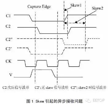
Figure 1: Issues in Asynchronous Reception Caused by Skew
2.3 Reset Strategies
The main issue with reset signals is Removal, which means ensuring that all flip-flops must exit the Reset state within the same clock cycle. Additionally, the timing of the completion of the Reset signal must not be too close to the clock edge to prevent flip-flops from entering metastability. Synchronous and asynchronous resets each have their advantages and disadvantages, and it is difficult to determine which one is superior. Aside from one issue mentioned in coding style, we will analyze and explain potential problems that may arise in both strategies.
Synchronous reset has the advantage that the reset occurs at the clock edge, which can prevent glitches in the reset signal. If the Reset signal is generated internally, it must ensure that the Reset pulse is sufficiently wide, at least 2 cycles, to allow the clock to sample it. However, this is also its disadvantage, as it requires an active clock and cannot reset some circuits during power-up. Moreover, synthesis may move the logic of synchronous reset to the D input of the flip-flop, treating it as a normal signal, which may lead to longer delays on the DataPath due to the transmission load and delay of the Reset signal.
Asynchronous reset’s primary benefit is that it does not require an active clock, which is essential for circuits needing power-on reset, such as buses. Additionally, unlike synchronous reset, the reset signal is not used as D input logic, resulting in a much cleaner DataPath. If there are glitches in the asynchronous reset, it may cause the chip to enter reset state. In this case, a two-stage DFF can be used to receive the Reset, followed by a tree to provide reset to the flip-flops, thereby eliminating glitches caused by inputs. If the design has multiple clock domains, two DFFs can be allocated for each clock domain to receive the Reset signal.
2.4 Gated Clocks
Gated clocks primarily reduce power consumption and area while simplifying logic to improve frequency. When coding, it is important to consider glitch-free gated signal designs. In DFT design, since the clock of the flip-flop is the output of the previous logic (other derived clocks have the same issue), testing such flip-flops requires adding a level of Mux to the clock. In normal operation mode, a derived clock is used, while in scan testing, the normal clock is adopted. The main issues with gated clocks arise during synthesis, CTS insertion, and STA analysis, which will be specially discussed later.
2.5 Bus Implementation
This section only discusses bus implementation methods, without involving bus protocols. When designing a bus, two basic choices must be made: whether to use a tri-state bus or a multiplexed bus structure. In full-custom designs, designers seem to prefer tri-state, as various components on the bus can be distributed across different parts of the chip. Additionally, since it can reduce the number of connections, it must ensure that no bus conflicts occur at any time. If multiple drivers can lead to serious errors, measures must be taken to eliminate this risk. For example, tri-state enables can be generated through a decoder to produce one-hot encoding to prevent logical errors and chip damage caused by multiple drivers. Meanwhile, tri-state buses must be connected to pull-up resistors to prevent uncertainty in bus data during periods of inactivity, while DC and other synthesis tools do not support this. Additionally, the capacitive load of tri-state buses is also a significant issue that adversely affects performance and area due to the load from multiple circuit units connected to the bus, and the bus layout itself brings some load. Finally, tri-state buses also pose difficulties for DFT design. For these reasons, in non-custom ASIC designs, it is unnecessary to choose a tri-state bus method. In contrast, the issue with multiplexers is the congestion caused by multiple connections, while the delay of the multiplexer is not a significant issue. In deep submicron designs, the differences in gate delays have become less pronounced, and multiple metal layers provide sufficient routing resources.
3. Logic Synthesis and Related Issues in Back-End Design
3.1 Coding Style Check
DC provides good support for coding style checks. Before performing logic synthesis, it is best to analyze the DC log files to see if there are any of the aforementioned or other coding style issues. The set_dont_use command can be used to prohibit the use of some process-related cells, and the all_registers command with parameters can report the latches used in the design. Below, we mainly discuss the special handling of some situations mentioned earlier during synthesis and back-end implementation. Additionally, many EDA tools provide coding style checks.
3.2 Asynchronous Clock Domains
In coding design, we separate asynchronous clock domain receiving modules into independent modules through partitioning, while other modules use a single clock, making synthesis constraints relatively simple. For those modules with asynchronous clock domains, if no constraints are applied, DC will always try to meet the setup/hold times of the sampling clock, while the designer does not care about these issues between asynchronous clock domains, and their metastability issues have already been resolved during coding. Typically, we can set the paths between asynchronous clock domains as false_path. For example:
set_false_path -from [get_clocks CLKB] -to [get_clocks CLKA]
If the control of asynchronous interface data is done in the last manner (i.e., reading data within the agreed cycle), the skew control of the sender’s data must also be within a certain range. Since these paths are not constrained (although we can set the Maxdelay for these paths, such constraints do not effectively control skew), tools cannot automatically optimize these paths. Therefore, it is best to use manual layout methods to keep these skews within a controllable range, and during the STA phase, these skews also need to be analyzed separately.
3.3 Special Handling of Clock Signals
Gated clocks, like all internal clocks, can cause hold time issues due to clock skew. By default, clock tree synthesis tools do not connect clock signals connected by logic gates to the clock tree, while clocks on non-gated flip-flops are connected to the clock tree. This clock delay is quite considerable. To control the skew between gated and non-gated clocks, it is common to take the clock signal from the upper level of the clock tree leaf nodes as the control clock input for the gates. During the STA phase, special analysis of the setup/hold times of gated clocks and glitch checks is required.
Next, we revisit the situation in Example 1’s code, which can be illustrated in Figure 2.

Figure 2: Using Clock as a Regular Signal
For discussion convenience, after clock tree insertion, assume there is a 1 cka cycle skew between A and B. As shown in Figure 3, if point A is used as the input to the adder, the resulting waveform is ckb’, while if point B is used as input, the resulting waveform is ckb. Clearly, based on Example 1’s code, ckb is the correct one. Therefore, it is crucial to note the potential issues that may arise when clocks are used as regular signals. There is no universal solution to these problems. In this example, not using signals from the clock tree is correct, but in other applications, signals from the clock tree must be used. For instance, if the clock is chosen based on the data latched by two flip-flops in CK, then the clock signal used as the selection signal must be pulled from the clock tree. Thus, if clock signals are used as regular signals in the design, special handling must be undertaken during back-end design.
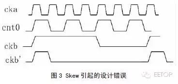
Figure 3: Design Errors Caused by Skew
If the design uses both the rising and falling edges of the clock, it is also necessary to use buffers that can balance the rising and falling edges during clock tree insertion to ensure a good duty cycle.
3.4 Reset Signals
The Removal issue in resets requires that for asynchronous reset signals, a tree must balance the skew at various load points. However, the skew control of reset signals is not as strict as that of clocks; as long as the Removal check is satisfied, it is acceptable. Tools like PT support Removal checks.
4. Gate-Level Simulation with Post-Layout Delay Information
Gate-level simulation is crucial as it serves as the final checkpoint, focusing on two aspects: functional verification and timing verification. The primary emphasis is on timing verification, while functional verification has already been largely covered at the RTL level. If equivalence verification passes, functional issues are generally resolved.
Timing simulation requires understanding the delay models used by simulation tools. The delay calculations of simulation tools are based on a simple delay model: CircuitDelay=TransportDelay+InertialDelay.
Timing simulation aims to use back-annotated SDF files to simulate situations that cannot occur at the RTL level, such as resets and state machine flips. Comprehensive verification should include checking the hold time of short paths under best-case conditions and the setup time of long paths under worst-case conditions. Although these issues are also checked in STA, gate-level simulation is still necessary, especially in designs using both edges of the clock. Additionally, for designs with asynchronous clock interfaces, adjustments to the phase relationship of asynchronous clocks are needed to check for potential synchronization failure issues. Special clock issues discussed in section 3.3 can also be verified for correctness through gate simulation. It is crucial to analyze the waveforms of key signals against expectations thoroughly.
5. Conclusion
ASIC design is a complex and holistic process that spans structural design, coding design, synthesis, physical design, timing analysis, and gate-level simulation. The entire process is lengthy, and each link cannot be considered in isolation. Designers must dedicate significant time to reduce or eliminate potential risks in the design to create products that are functionally correct and meet performance requirements.
Appendix: Typical ASIC Design Process (Detailed)
1) Structural and electrical specifications. 2) RTL-level code design and simulation test platform file preparation. 3) Insert BIST (Design For Test) for modules with storage elements. 4) Perform dynamic simulation of the complete design to verify functionality. 5) Set up the design environment, including the design libraries used and other environment variables. 6) Use Design Compiler tools to constrain and synthesize the design, and add scan chains (or JTAG). 7) Use the static timing analyzer built into Design Compiler to perform module-level static timing analysis. 8) Use the Formality tool for formal verification of RTL and synthesized gate-level netlists. 9) Perform static timing analysis of the entire design using PrimeTime before layout and routing. 10) Annotate timing constraints to the layout tools. 11) Layout of timing-driven cells, clock tree insertion, and global routing. 12) Insert the clock tree into the original design of DC. 13) Use Formality for formal verification of synthesized netlist and netlist with inserted clock tree. 14) Extract estimated timing delay information from the layout after global routing. 15) Back-annotate estimated timing delay information to Design Compiler or Primetime. 16) Conduct static timing analysis in Primetime. 17) Optimize design in Design Compiler. 18) Perform specific routing for the design. 19) Extract actual timing delay information from the routed design. 20) Back-annotate the extracted actual timing delay information to Design Compiler or Primetime. 21) Conduct post-layout static timing analysis in Primetime. 22) Optimize design in Design Compiler (if necessary). 23) Conduct gate-level simulation with timing information post-layout. 24) Perform LVS and DRC verification, then tape-out.
Follow EETOP, input Qianbao Box in the background to see more articles related to digital IC & ASIC & FPGA:
-
Classic Details of ASIC Front-End and Back-End Design
-
Introduction to Chip Area Estimation Methods
-
Insights from ASIC Experts
-
Basic Circuit Design in Verilog (Including: Clock Domain Synchronization, Seamless Switching, Asynchronous FIFO, Debounce Filtering)
-
Overview and Review of Digital Front-End and FPGA Design Related Literature
-
Learning Process for Digital IC Design
-
Design Ideas for Clock Switching Circuits to Prevent Glitches
-
Brief Introduction to Function Generator Implementation Methods
-
Implementing Simple UDP/IP Communication with FPGA (Using Pure Hardware Language, Not Soft Core)
-
Introduction to Digital Integrated Circuit Design — From HDL to Layout
-
Design of Synchronizers
-
Skill Tree for Digital IC Engineers
-
Microelectronics Tree
-
Overview and Tools of Complete IC Design Process
-
IC Chip Design and Production Process
-
Where Does the Cost of IC Chips Come From?
-
Discussing Chip Design
-
Thoughts on IC Design
-
Complete Process of Digital IC Design (Very Detailed!)
-
Global View of Digital IC Design Technology (110-page PPT!)
-
Key Considerations in ASIC Design Stages
-
In-Depth Discussion on Setup and Hold
-
Discussion on Setup Time and Hold Time
-
Negative Values of Setup and Hold in Static Timing Analysis
-
Entry Points and Methods for Static Timing Analysis (STA)
-
Basics and Applications of Static Timing Analysis (STA)
-
Glitch Phenomenon in Combinational Logic Design
-
What is the Career Outlook for Digital IC Design Engineers?
-
Knowledge Structure of a Qualified Digital IC Design Engineer
-
RS Codec Verilog Code RS(255,247)
-
RS(255,239) Codec Algorithm, Verilog Code, and Detailed Explanation
-
Very Detailed Verilog Tutorial, 472 Pages
-
A Simple 8-bit Processor Complete Design Process and Verilog Code
-
Experience Sharing from Netizens: Verilog Design Cautions
-
An Example of Synchronous and Asynchronous Timing in Verilog
-
Summary of Semiconductor and Microelectronics English Vocabulary
-
Introduction to Spectre Verilog Mixed-Signal Circuit Simulation Methods Using DAC as an Example
-
The Friendship Between IC Design and Verification Engineers Can Flip at Any Moment
-
Basic Process and Tools Used in Digital IC Design
-
Foreign Digital IC Interview Questions (Very Detailed, with Answers)
-
Understanding and Utilizing Timing Reports
-
Asynchronous FIFO Design (Very Detailed, Illustrated, Worth Reading!)
-
Chasing Parallel Universes — Design of Asynchronous FIFO Controllers
-
Why Use Gray Code in Asynchronous FIFO?
-
Classic 100 Questions for Digital IC Design Engineer Written Exams and Interviews (1~50)
-
Classic 100 Questions for Digital IC Design Engineer Written Exams and Interviews (51~100)
-
Synchronous/Asynchronous Design and Metastability
-
Discussing FPGA/CPU/PCIe/Cache-Coherency/CAPI
-
How Does FPGA Achieve 30 Times Speed Cloud Acceleration? What Has Been Accelerated?
-
Understanding the Development Path of FPGA
-
[Insights] Tencent Cloud FPGA Deep Learning Algorithms
-
Machine Learning in the Cloud: Deep Neural Networks on FPGA
-
Netizen Complaints: 9 Years of FPGA Work Summary, Bitter Sea with No End, Poor Life
-
FPGA Digital Circuit Design Experience Sharing (Insights!)
-
[Insights] Low-Speed Protocol Design Experiment Manuscript and Source Code Based on FPGA
-
Advanced FPGA Design
-
Principles and Algorithms of CRC Cyclic Redundancy Check and FPGA Implementation
-
Discussion on Inconsistencies Between FPGA Design Simulation and Hardware Testing
-
How to Extend the Operating Temperature Range of FPGA?
-
How to Digitize Hundreds of Signals Using a Single Xilinx FPGA Chip?
-
A Summary of an FPGA Engineer’s Personal Work Experience
-
Making FPGA Visual Functions Popular
-
Introduction to FPGA Power Supply
-
FPGA Division Operation Implementation
-
Using FPGA-Based Fuzzy Controllers to Control Sugar Extraction
-
Designing High-Performance USB Devices Using Artix-7 FPGA
-
FPGA Application Article: Testing New Memory Technology Chips Using Zynq SoC
-
AES 128-bit Encryption and Decryption Algorithm Based on XILINX FPGA
-
Efficient Parallel Real-Time Upsampling Implementation Using Xilinx FPGA
-
FPGA Practical Exercises Logic Part (1) – FPGA vs ASIC, FPGA vs CPLD, VERILOG vs VHDL
-
FPGA Practical Exercises Logic Part (2) – Applications and Advantages of FPGA, FPGA Development Process
-
FPGA Practical Exercises Logic Part (3) – Five Elements of FPGA Board-Level Circuit Design
-
Performance Comparison of CRC Algorithms Based on ARM and FPGA
-
How to Prevent FPGA Projects from Going Astray
-
Zynq On-Chip XADC Application Notes
-
Zynq Device Clock Subsystem Introduction
-
Understanding Setup and Hold Times, and Their Margins
-
C Programming Experience and Skills for Soft Core MicroBlaze
-
Application of Tcl in Vivado
-
Detailed Introduction to Vivado Usage 1: Creating Projects, Writing Code, Behavioral Simulation, Testbench
-
Detailed Introduction to Xilinx Vivado Usage (2): Synthesis, Implementation, Pin Assignment, Clock Settings, Programming
-
Introduction to Vivado Usage 3: Using IP Cores
-
Xilinx FPGA Getting Started Series 1: Installing ISE14.6
-
Xilinx FPGA Getting Started Series 2: Installing Modelsim SE 10.1
-
Xilinx FPGA Getting Started Series 6: Associative Settings for ISE and Modelsim Joint Simulation
-
Xilinx FPGA Getting Started Series 7: Creating a New Project
-
Xilinx FPGA Getting Started Series 8: Creating and Editing Verilog Source Files
-
Xilinx FPGA Getting Started Series 9: Verilog Syntax Check
-
Xilinx FPGA Getting Started Series 10: Modelsim Simulation Verification
-
Xilinx FPGA Getting Started Series 11: Overview of PWM Buzzer Driver Functionality
-
Xilinx FPGA Getting Started Series 12: PWM Buzzer Driver Pin Assignment
-
Xilinx FPGA Getting Started Series 13: PWM Buzzer Driver Synthesis, Implementation, and Configuration File Generation
-
Follow Me to Start Learning FPGA from Scratch (One Week Series): Day One: Verilog Syntax
-
Follow Me to Start Learning FPGA from Scratch (One Week Series): Day Two: Combinational Logic Design
-
Follow Me to Start Learning FPGA from Scratch (One Week Series): Day Three: Sequential Logic Design
-
Follow Me to Start Learning FPGA from Scratch (One Week Series): Day Four:
-
Follow Me to Start Learning FPGA from Scratch (One Week Series): Day Five: Blocking and Non-Blocking
-
Follow Me to Start Learning FPGA from Scratch (One Week Series): Day Six: Finite State Machines
-
Follow Me to Start Learning FPGA from Scratch (One Week Series): Day Seven: Designing a CPU with Only 4 Instructions
-
FPGA Getting Started Series One: 0 and 1 – The Wonderful World Begins Here
-
FPGA Getting Started Series Two: Experiences in Learning Verilog/VHDL Syntax
-
FPGA Getting Started Series Three: Revealing Surface Phenomena – Logic Relations
-
FPGA Getting Started Series Four: Exploring Inner Essence – Device Structure
-
FPGA Getting Started Series Five: The First Engineering Example
-
Detailed Introduction to Vivado Usage 2: Synthesis, Implementation, Pin Assignment, Clock Settings, Programming
-
Design of Multi-Port Read and Write Storage Management Based on FPGA
-
Implementing Oberon System on Low-Cost FPGA Development Board
-
Fully Programmable Abstraction: You Control Your Programming
-
Tips for Using FIFO Based on XILINX FPGA
-
How to Handle Multiple Image Sensors in Intelligent Vision Systems?
-
FPGA Clock and Reset Circuit Design
-
In FPGA Design, Timing is Everything
-
In FPGA Design, Timing is All
-
Using FPGA to Characterize Large-Scale MIMO Channels
-
How to Port PetaLinux to Xilinx FPGA
-
Discussion on Inconsistencies Between FPGA Design Simulation and Hardware Testing
-
Where is FPGA Suitable? What Role Do OpenCL, C, and C++ Languages Play in FPGA and Full SoC?
-
Beginner’s Guide: INOUT Interfaces and High-Impedance States in FPGA
-
Science Popularization: The Design and Manufacturing Process of HiSilicon CPUs, After Watching This, You Will Realize Huawei’s Hard Work
-
Books Related to Processor IC Design Most Loved by Netizens
-
Insights: Global View of Digital IC Back-End Design — What Does Digital Back-End Do from RTL to GDS (137-page PPT)
-
Science Popularization: The Design and Manufacturing Process of HiSilicon CPUs, After Watching This, You Will Realize Huawei’s Hard Work
-
CPU DIE Photo Collection
-
Popular Science: The Evolution of CPUs (X86 Edition)
-
A Story from Aspiring to CPU Design from University to Realization After Graduation!
-
Finally Cleared Up, After Reading This You Can Design CPUs Too
-
Science Popularization: How GPUs Work? What are the Differences with CPUs and DSPs?
-
How Did ARM Overcome MIPS in CPU IP Licensing?
-
From Sand to Chip, Let’s See How CPUs are Manufactured
-
In-Depth Analysis of Domestic Longxin New Architecture CPU
-
Review of Open-Source Processors and SoC Research Based on RISC-V Architecture
-
RISC-V and DSA! Transcript of Computer Architecture Masters Patterson and Hennessy’s Speech
-
Comprehensive RISC-V Resources in Chinese!
-
Science Popularization: Comparison of ARM and X86 CPU Architectures
-
From Zero to Mastery — The Path of Processor (CPU) Design
-
Discussing the Differences Between CPUs and GPUs
-
Designing Specialized Processors by Yourself

Click to Read the Original Text to View Related Blogs