

ASIC (Application Specific Integrated Circuit) chips are application-specific integrated circuits designed from the ground up to meet the specific needs of users for certain electronic systems. Their computational power and efficiency can be customized according to algorithm requirements, making them the product of fixed algorithm optimization design. ASIC chip modules can be widely used in artificial intelligence devices, cryptocurrency mining equipment, consumables printing devices, military defense equipment, and other smart terminals.
At the hardware level, ASIC chips are composed of basic silicon materials, gallium phosphide, gallium arsenide, gallium nitride, and other materials. At the physical structure level, ASIC chip modules are assembled from external memory units, power managers, audio and video processors, network circuits, and other IP cores. The same chip module can carry one or several ASIC chips with the same or different functions to meet one or more specific needs.
(1) According to the degree of customization, ASIC chips can be divided into fully customized ASIC chips, semi-customized ASIC chips, and programmable ASIC chips.
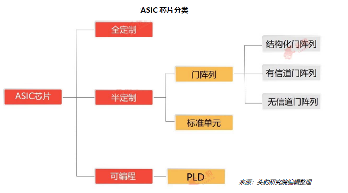
Fully customized ASIC chips are among the highest degree of customization, where researchers design logic units for different functions based on various circuit structures, building analog circuits, memory units, and mechanical structures on the chip board. Logic units are connected via masks, and the masks for ASIC chips also feature high customization.
The design cost for fully customized ASIC chips is relatively high, with an average design time of over 9 weeks per chip module. This type of chip is typically used for advanced applications.
Compared to semi-customized ASIC chips, fully customized ASIC chips perform excellently in aspects like performance and power consumption. For the same function, under the same process, fully customized ASIC chips have an average computational power output about 8 times that of semi-customized ASIC chips. A fully customized ASIC chip using a 24nm process outperforms a semi-customized ASIC chip using a 5nm process.
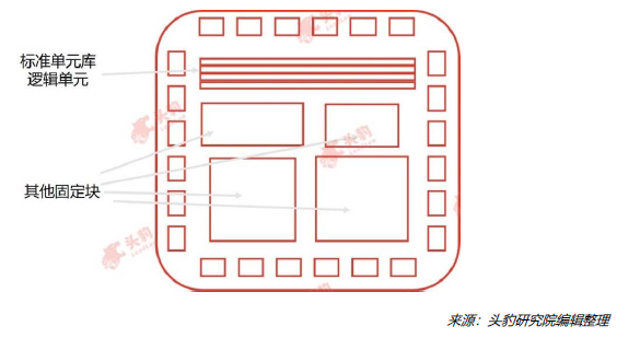
The logic units that make up semi-customized ASIC chips are mostly derived from a standard logic unit library, with some customized designs based on specific needs. The design cost is lower and flexibility is higher compared to fully customized ASIC chips.
Gate array ASIC chips include channel gate arrays, non-channel gate arrays, and structured gate arrays. In gate array ASIC chips, the positions of transistors on the silicon wafer are predetermined and cannot be changed. Designers typically adjust the interconnection structure of logic units by changing the metal layers at the bottom of the chip.
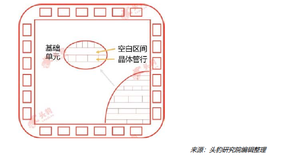
Channel Gate Array ASIC Chips:These chips have highly fixed transistor positions, allowing designers to layout circuits in predefined blank spaces between transistor rows;
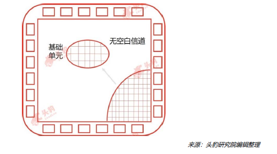
Non-Channel Gate Array ASIC Chips:In a non-channel structure, there is no space for circuit layout between transistor rows, so designers typically route above the gate array units;
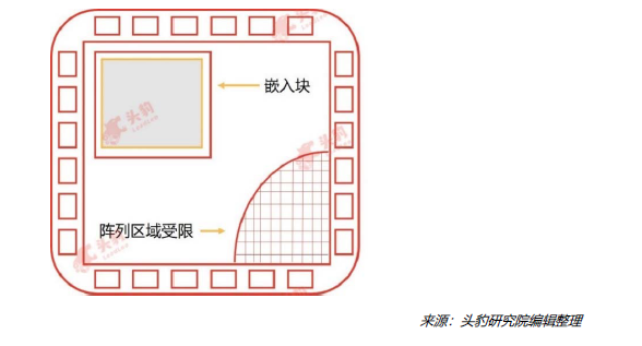
Structured Gate Array ASIC Chips:This structure includes basic gate array rows and embedded blocks. The embedded blocks can enhance the flexibility of line layout but impose size restrictions on the chip. Under this structure, the area usage efficiency of line layout is high, design costs are low, and turnaround times are short.
b. Standard Cells
These ASIC chips are composed of logic units selected from a standard cell library. Designers can arrange standard cells according to algorithm requirements. In addition to standard cells, fixed blocks such as microcontrollers and microprocessors can also be used in standard cell ASIC chip architectures.
③ Programmable ASIC Chips
Broadly speaking, programmable ASIC chips can be divided into FPGA chips and PLD chips. In actual production, the number of research institutions and enterprises that classify FPGA chips as different from ASIC chips is increasing, so this report only considers PLD (Programmable Logic Device) as a subclass of programmable ASIC chips.
PLD, also known as programmable logic devices, structurally includes basic logic unit matrices, flip-flops, latches, etc., with their interconnection part existing as a single module. Designers program the PLD to meet some customized application requirements.
① TPU stands for Tensor Processing Unit, specifically designed for machine learning. For example, Google developed a programmable AI accelerator for the Tensorflow platform in May 2016, which can run when the internal instruction set changes or updates algorithms.
② BPU stands for Brain Processing Unit, an embedded AI processor architecture proposed by Horizon Robotics.
③ NPU stands for Neural Processing Unit, which simulates human neurons and synapses at the circuit level and directly processes large-scale electronic neuron and synapse data using deep learning instruction sets.
Traditional chips like CPUs read and execute external program code instructions to generate results, whereas ASIC chips read raw input data signals and directly generate output signals after computation through internal logic circuits.
Compared to CPUs, GPUs, and FPGAs, ASIC chips have multiple advantages in dedicated system applications, specifically in the following aspects.
① Area Advantage:ASIC chips are constructed in a purely digital logic circuit form, avoiding redundant logic units, processing units, registers, and memory units during design, which helps to reduce chip area. For small-area chips, more chips can be cut from the same specification wafer, assisting companies in reducing wafer costs.
② Energy Consumption Advantage:ASIC chips consume relatively less power per unit of computational power compared to CPUs, GPUs, and FPGAs. For instance, GPUs consume about 0.4 watts of power per unit of computational power on average, while ASICs consume about 0.2 watts, making them more suitable for the energy constraints of new smart appliances.
③ Integration Advantage:Due to customized design, the systems, circuits, and processes of ASIC chips are highly integrated, helping customers achieve high-performance integrated circuits.
④ Price Advantage:Due to their small size, high operating speed, and low power consumption, ASIC chips are priced significantly lower than CPUs, GPUs, and FPGAs. Currently, the average price of ASIC chips in the global market is about $3, and if they reach mass production scale in the future, their prices are expected to continue to decline.
① The high degree of customization of ASIC chips leads to long design and development cycles, requiring physical design and reliability verification, which results in slower time-to-market.
② ASIC chips have a high dependency on algorithms. Rapid updates and iterations of artificial intelligence algorithms lead to a high frequency of ASIC chip updates.
③ Due to the high degree of customization, the long R&D cycle increases the risk of ASIC products being eliminated from the market.
① Google launched the TPU in 2016, embedding 4 TPUs in the 2017 version of the AlphaGo physical processor, which supports the Google Cloud TPU platform and machine learning supercomputers.
② IBM simulated brain structures and launched the second-generation TrueNorth chip with a 28nm process in August 2014, which can be applied to real-time video processing.
③ Intel launched the Xeon series ASIC chips in 2017. This series of chips can act as processors independently, without additional host processors or auxiliary processors, and can be applied to deep learning.
④ Stanford University launched an ASIC chip based on a new neuromorphic computing architecture, achieving computation speeds 9,000 times that of ordinary computers, capable of simulating about 1 million brain neurons and billions of synaptic connections.
⑤ Emerging tech companies are expanding the application of ASIC chips into fields such as security, assisted driving, traditional home appliances, and smart healthcare.
References:China ASIC Chip Industry Premium Report

<Complete Knowledge of Server Basics (Ultimate Edition)>, comprehensive coverage of content, in-depth explanation of knowledge points, providing a complete 182-page paid download.
How to Obtain:Click “Read the Original” to view details, providing PPT editable version and PDF reading version.
Warm Reminder:
Please search for “AI_Architect” or “Scan” to follow the public account for real-time access to deep technical sharing. Click “Read the Original” to get more exciting technical content.