Recently, I have started to relearn the common interface protocols used in my work, and I would like to share them for everyone’s reference~
I2C (Inter-Integrated Circuit) is a serial communication protocol developed by Philips (now NXP) in the 1980s, primarily used for short-distance, low-bandwidth communication on a board, such as the connection between sensors, EEPROM, and other peripheral devices with microcontrollers. It is a multi-master, multi-slave, synchronous, half-duplex protocol.I3C (Improved Inter-Integrated Circuit) is an upgraded version of I2C launched by the MIPI Alliance in 2016, aimed at addressing the limitations of I2C, such as low speed, high power consumption, and lack of support for dynamic addressing. It is backward compatible with I2C, supporting higher speeds, lower power consumption, and advanced features such as in-band interrupts and dynamic address assignment.I3C is commonly used in modern mobile devices, IoT, and sensor networks.
The main PINs and functions of I2C and I3C
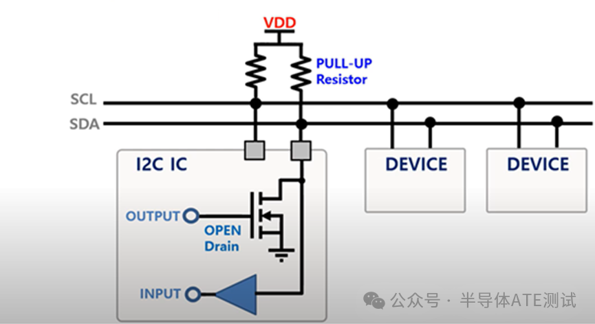
I2C and I3C both use two wires (two buses), making them simple and pin-efficient. Both share the same physical interface, but I3C has undergone relevant optimizations in electrical characteristics to improve efficiency (such as changing from open-drain to push-pull output). The internal interface circuits for I2C & I3C are shown in the figure below:
-
The main PINs of I2C
-
SDA (Serial_Data_Line): Serial data line for transmitting data(DATA), address(Address), and acknowledgment signals(ACK)
-
Function: Used to transmit data to the target device or receive data from the target device. For example:🌰: The controller can send configuration data and output codes to the target Digital-to-Analog Converter (DAC) or receive conversion data from the target Analog-to-Digital Converter (ADC).
-
Circuit structure: Open-drain/ open-collector design, meaning the device can only pull the level low (output0), and the high level of SDA is provided by an external pull-up resistor. This is like a “shared pull rope”: any device can pull it low, but when released, it is pulled high by the resistor.
-
SCL (Serial Clock Line) : Serial clock line, providing a synchronous clock signal
-
Function: Controlled by the controller device, used to synchronize the data input/output clock of the target device, controlling the rhythm of data transmission to ensure synchronization
-
Circuit structure: Open-drain design, where the master device generates the clock, and the slave device follows
-
Other auxiliary:GND (ground) and VCC (power), but not core to the protocol. The bus requires external pull-up resistors (typically1-10kΩ) connected to VCC to maintain a high level when idle.
-
The main PINs of I3C
-
SDA: Similar to I2C, but supports push-pull output (push-pull), allowing devices to actively pull high or low, improving speed and power efficiency. Function: Transmit data, address, commands, and interrupt signals (In-Band, Interrupt, IBI)
-
SCL: Clock line, similar to I2C, but the I3C master device can dynamically switch modes. Function: Synchronize clock, supporting higher frequencies.
-
Compatibility:I3C bus can mix with I2C devices (legacy_I2C_slaves), but attention must be paid to voltage and speed matching. I3C introduces dynamic addressing (Dynamic Address Assignment), eliminating the need for fixed address jumpers.
I²C & I3C use half-duplex communication mode, where only one controller or target device can send data on the bus at the same time. In contrast, the Serial Peripheral Interface (SPI) uses a full-duplex protocol, allowing simultaneous bidirectional data transmission. SPI requires four communication lines: in addition to the serial clock line, it also needs dedicated chip select lines to select communication devices, and two lines for data input and output for the target device.
I²C controllers are responsible for initiating and terminating communication, thereby eliminating the risk of bus contention. By communicating with the unique address of the target device, it enables an architecture that connects multiple controllers and multiple target devices on the I²C bus simultaneously.
All devices’ SDA and SCL lines are connected to the bus using an open-drain structure, which requires pull-up resistors connected to a common voltage source.
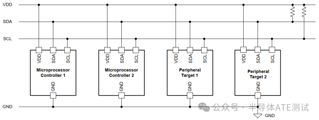
Open-Drain Connection
SDA and SCL lines both use an open-drain connection structure, connected to NMOS transistors. The open-drain connection pulls down or releases the communication line level by controlling the NMOS transistor’s on/off state. “Open-drain” specifically refers to the bus connection state when the NMOS transistor is in the off state. The following figure shows the open-drain connection state when the NMOS transistor is on.
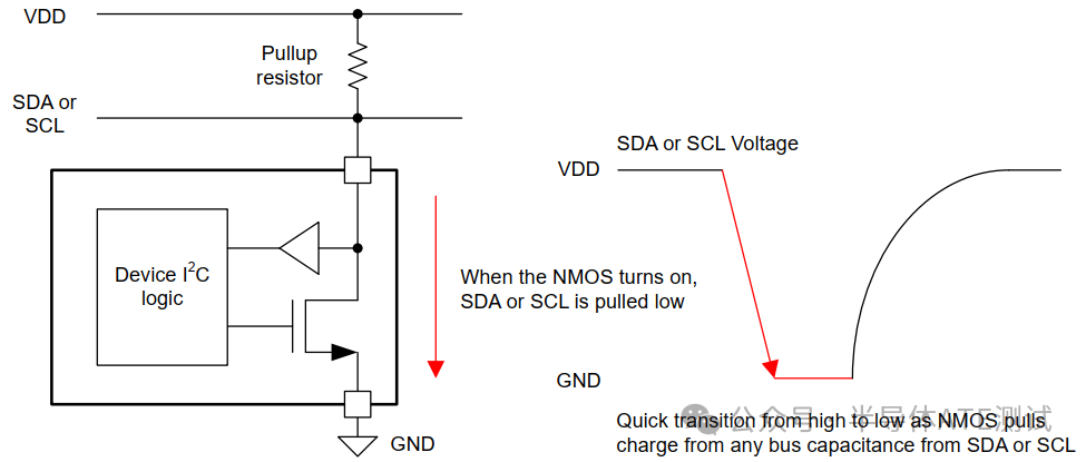
By controlling the NMOS transistor’s on/off state, the levels of the SDA or SCL lines can be set. When the NMOS transistor is on, the device discharges current to ground through the resistor, thus pulling the open-drain line low. Typically, due to the NMOS transistor’s pull-down effect on the SDA or SCL line, the transition speed from high to low is very fast (this is also why OD circuits are widely used in falling edge-triggered protocols), and the transition rate depends on the NMOS transistor’s driving capability and the bus capacitance.
When the NMOS transistor is off, the device stops discharging current, and the pull-up resistor pulls the SDA or SCL line to a high level (VDD). The following figure shows the open-drain line state when the NMOS transistor is off. At this time, the pull-up resistor pulls the line high, but due to the need to overcome the bus capacitance charging process, the level transition speed is slower (non-active driving mode).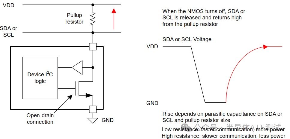
By controlling this open-drain connection, the SDA and SCL lines can switch between high and low levels, thus completing I²C communication.
Due to the presence of capacitance in the I²C communication lines, the discharge process of the SDA and SCL lines exhibits an exponential RC time constant characteristic, with specific values depending on the pull-up resistor’s resistance and the bus capacitance. Larger capacitance will limit the I²C communication speed, the number of devices that can be connected, and the physical distance between devices. Smaller resistance pull-up resistors can speed up the rise time but will increase power consumption; larger resistance pull-up resistors can reduce power consumption but will slow down the rise time, leading to a decrease in communication speed.
I2C Protocol Speeds
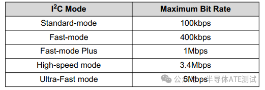
I²C includes multiple speed modes, initially with a maximum transmission rate of 100kbps in the Standard Mode (Sm). Subsequently, the rate was increased to 400kbps in Fast Mode (Fm), which can be used when the bus capacitance and driving capability meet the requirements. Sm & Fm are the most widely used modes.
In addition to these two modes, with the development of communication technology, there is also: Fast Mode Plus (Fm+) supporting a maximum communication rate of 1Mbps. Achieving this rate requires the device driver to have stronger driving capability to meet stricter rise/fall time requirements.
The Standard Mode Sm, Fast Mode Fm, and Fast Mode Plus Fm+ all use the same communication architecture, but the timing specifications differ for each mode, and the I²C hardware implementation in devices must adapt to different speeds.
I²C also includes two higher-speed modes:
-
High-Speed Mode (Hs-mode): supports a maximum data transmission rate of 3.4Mbps. In this mode, the controller must first send a specific control code to activate the target device’s high-speed transmission capability, and sometimes active pull-up is required to drive the communication lines.
-
Ultra-Fast Mode (UFm) is the highest-speed operating mode, supporting a maximum transmission rate of 5Mbps. This mode only supports write operations and omits some functions in the I²C protocol.
I2C and I3C Protocol Frames
I²C protocol communicates through frame structures. The controller device sends a start signal and first transmits the address frame, followed by one or more data frames consisting of single bytes. Each frame contains an acknowledgment bit to confirm that the target device or controller has successfully received the communication. The following figure shows the structural diagram of two sets of I²C communication frames.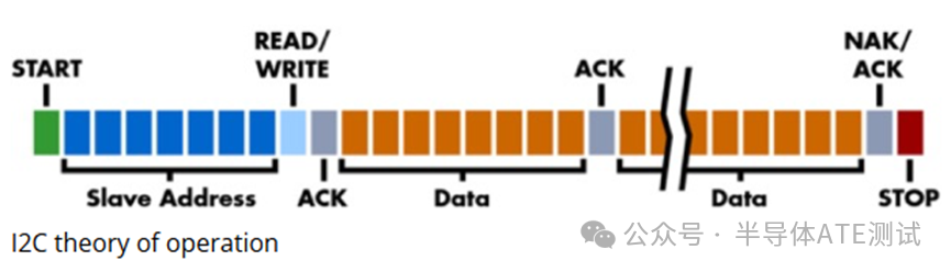
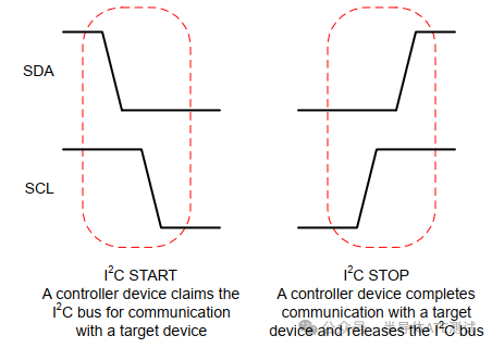
In the address frame’s initial phase, the controller device first generates a START condition: first pulling the SDA line low, then pulling the SCL line low. This operation allows the controller to monopolize the bus control, avoiding competition with other controllers. Each I²C target device has a corresponding unique address, and the controller uses the target device address for data transmission in subsequent frames. I²C addresses use 7-bit encoding, theoretically allowing for 2⁷ (i.e., 128) independent addresses, but some reserved addresses practically limit the number of available devices.
The 8th bit of the address frame is the read/write control bit (R/W)
-
If this bit is 1, it indicates that the controller requests to read data from the target device;
-
If it is 0, it indicates a request to write data.
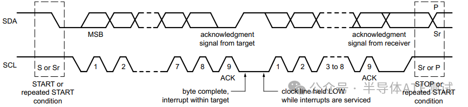
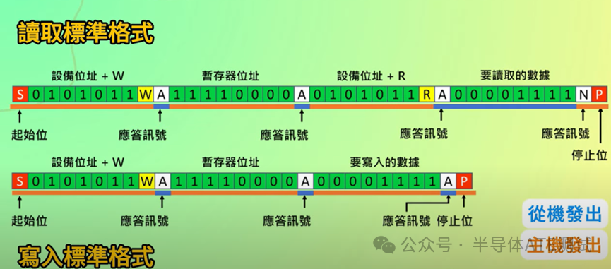
Each communication byte is followed by an additional bit to verify successful transmission, called Ack. After the address byte transmission ends, the target device pulls the SDA low during the SCL pulse as an acknowledgment (ACK), indicating successful reception of the address. If this bit remains high (NACK), it indicates no device responded to the address, and communication has failed.
After the address frame, multiple data frames can follow, transmitting in single bytes. Each data byte transmission is followed by an ACK response: when writing data, the target device pulls the SDA low to confirm, and when reading data, the controller pulls the SDA low to confirm. The ACK mechanism is an important debugging tool, and its absence may indicate that the target device did not recognize the address or that the controller did not receive the expected data.
After communication ends, the controller generates a STOP condition: first releasing the SCL line and then releasing the SDA line, declaring the communication complete and releasing bus control.
Happy Birthday to Mom 🎂🎂🎂~