The first thing to focus on when designing a chip is its PPA (Performance, Power, Area). This article discusses the second P, Power consumption, and how to achieve low power design in RTL, which is crucial for the battery life of mobile devices. Don’t let your chip unnecessarily increase power consumption.
Data Path Register Sampling
Data registers can sample with vld and without reset logic, which saves wiring area for the reset circuit of the registers. Additionally, the tools will automatically insert clock gating for the registers, achieving a reduction in power consumption.As for registers without reset, some beginners may find this concept challenging. How can registers not be reset? Wouldn’t that lead to x-state, causing system chaos? Yes, registers without reset can produce x-state, but here we are talking about the data path, where all signals in the control path must have reset logic. In the data path, as long as the vld is valid when you use it, it doesn’t matter if it is x-state or other invalid data. The control path signals control the operation of the system; if x-state occurs, it will definitely hang. The data path only needs to ensure that the vld is effective, meaning that when I access this data, it is correct, regardless of whether it is x-state or other invalid data.Of course, if the data is used for control logic, this data must be reset.In the code example, the sequential logic can omit else; registers default to hold, while combinational logic must include else. vld is a pulse that directly pushes this data into the register for storage, and this register will hold this data until the next pulse arrives.
always @(posedge clk)begin if(data_vld) dout[63:0] <= din;end
Manual Clock Gating Insertion
Manual clock gating insertion can automatically turn off the clocks of certain modules based on different control scenarios, leaving a software control channel for software to shut down. This can effectively reduce dynamic power consumption.For example, when a calculation circuit is configured to be fully on, it requires four identical computation modules to work simultaneously. In the minimal case, only one module needs to work; thus, based on different configurations, the clocks of the other three modules can be turned off to reduce dynamic power consumption.
Entire Top Module Power Down
The entire secondary Top module can enter sleep mode, and after power down, all necessary data is written to memory. When the module is awakened and powered on again, the data is written back to the hardware. In ASICs, RAM can generate the functionality to determine whether to power down and save data; unnecessary dedicated storage RAM can also be powered down.If there are few registers for data use and storage, interfaces can be extended from the module to the top level, allowing software to read them. When the module is awakened and powered on again, the registers can be reconfigured back to the module through software. This is the low power mode.
Static Power and Dynamic Power
Static power exists as long as the circuit is powered; it cannot be avoided unless powered down. Dynamic power exists whenever there is a high-low level transition. In RTL design, a good coding style can also reduce dynamic power consumption; multipliers, adders, and other computational units can achieve reduced dynamic power by minimizing combinational logic flipping.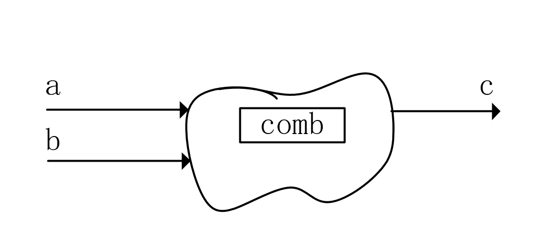 From input to output, if the values of combinational logic’s a and b remain unchanged, there is no level transition, so there will be no dynamic power, only static power. In design, consider the issue of invalid transitions in combinational logic; if a portion of data is invalid for a certain time, using enable signals to select this part of the logic to hold can effectively avoid dynamic power consumption.
Conclusion
This article records these points for now. For more discussions, feel free to leave comments. Let’s chat next time. Thank you all for your attention and support (sharing, liking, and appreciation). See you in the next article.