 👆If you wish to meet regularly, feel free to star 🌟 and bookmark it~
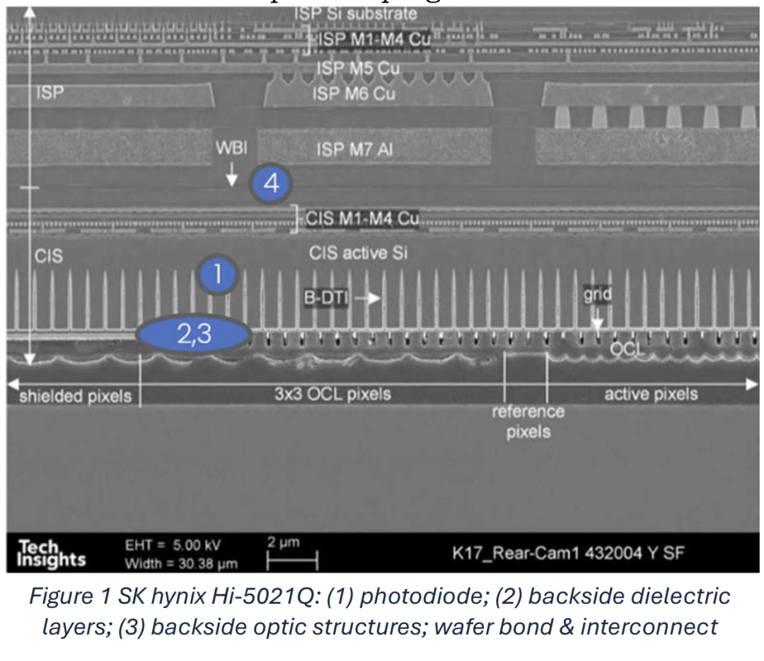
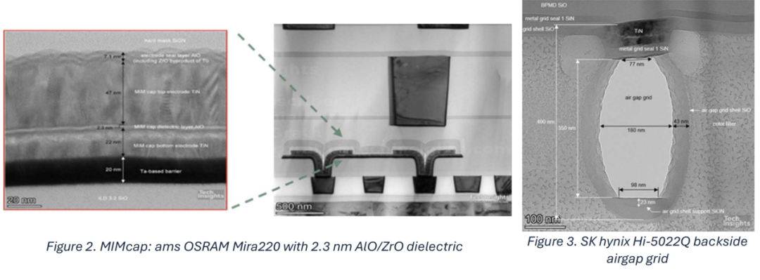
Over the past fifty years, the trajectory of pixel development has continuously increased the complexity of processes to achieve the performance required for imaging. In this process, the contributions of process engineers in development and manufacturing have been invaluable, successfully implementing a series of process improvements for image sensors to meet requirements in performance, yield, and cost. These improvements include the use of new materials to reduce crosstalk, enhance optical performance, and support additional functionalities (Figure 1). These processes can be adapted from other products (e.g., MIM caps, Figure 2) or can adopt novel structures, such as air gap back gates (Figure 3), applied to image sensors.
The product development process is accompanied by a series of technical challenges until market demands are met (e.g., reducing pixel size to lower costs and increase array size), then shifting to the next market demand (e.g., adding high dynamic range functionalities). The purpose of reverse engineering is to document the technological developments adopted by each manufacturer and to predict upcoming decision points in process development.
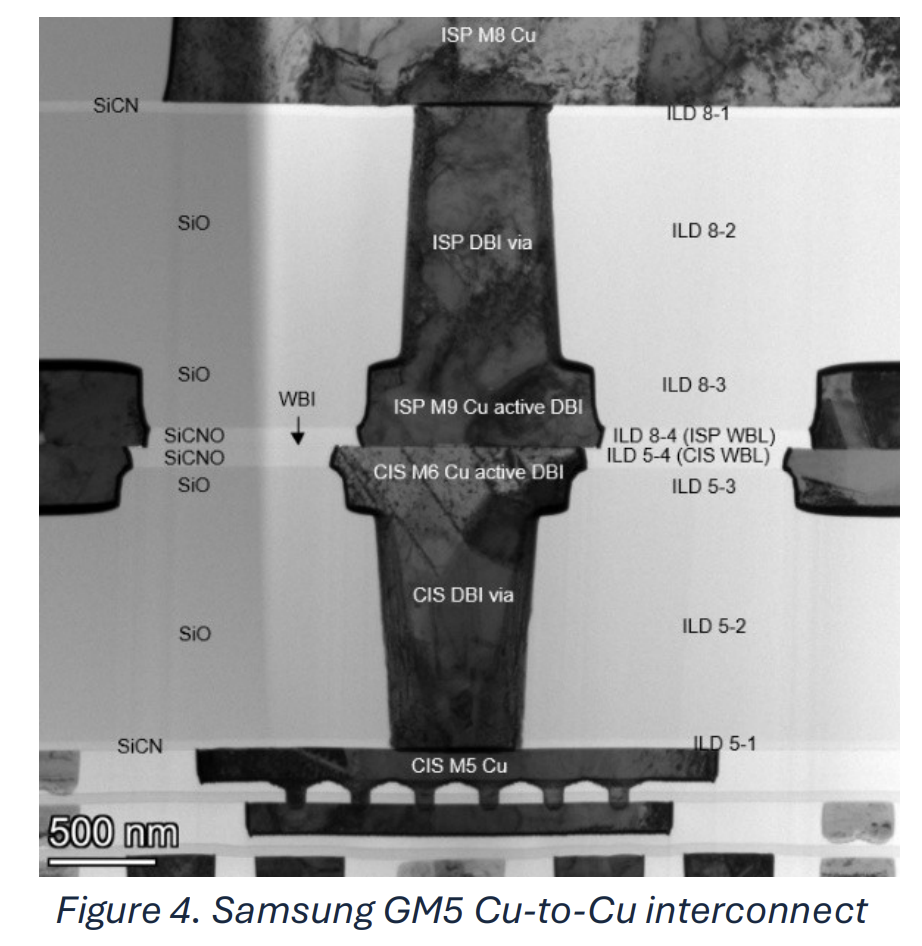
Stacking technology is an example of an enabling technology. Its development trajectory has evolved from front-illuminated single-metal CCDs to multi-metal CMOS (to increase functionalities), then to back-illuminated CMOS (to improve optical response), and finally to face-to-face stacked CMOS (to increase image processing capabilities while limiting chip size). The latter technology requires metal interconnects, initially achieved through silicon vias located at the chip edges, but is now being replaced by hybrid bonding, which utilizes the properties of materials: two polished SiO surfaces form cross-links upon contact, enhancing strength; two polished Cu surfaces also form cross-links, providing electrical interconnects. In fact, the SiO surface can simply be the dielectric layer for body interconnects. However, other foundries have found it useful to first form a layer containing C or N, and then form a thin SiO layer for bonding through plasma treatment (Figure 4).
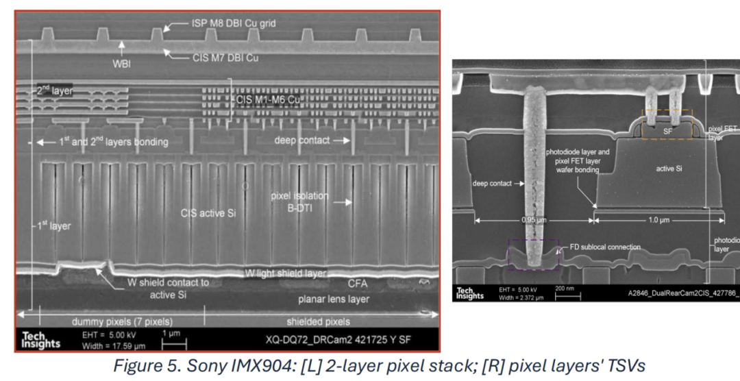
The next logical direction for pixel-level interconnect in stacked image sensors is a three-layer structure. This means that pixel layers can be partitioned to optimize photodiodes, making them independent of CMOS-related limitations, or separating the image signal processing layer to provide a pixel-level signal processing array layer, or adding a storage layer. The presence of an intermediate layer necessitates the development of interconnects from the back to the front of the wafer, whether by forming deep contact silicon vias from one side (Figure 5) or providing back-side copper pads for hybrid bonding interconnects.
The trend in wafer-to-wafer interconnect spacing has been steadily decreasing due to technical limitations, stabilizing before 2020. Since then, foundries have gradually stabilized the spacing, with each having its own optimal process parameters. TSMC appears to be the most competitive at a spacing of 1.4µm.
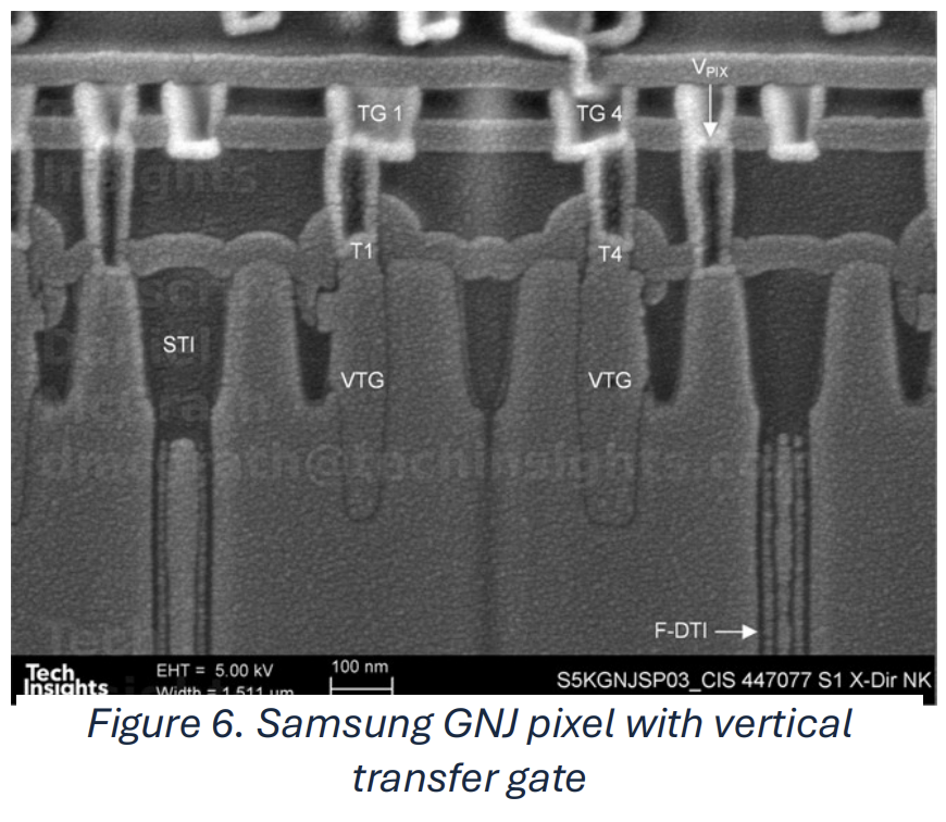
The optimal size for smartphone image sensors seems to be 50 million pixels, with a pixel pitch of 0.5µm to 0.7µm. Technically, there are differences in the choice of planar or vertical transfer gates, as well as the implementation of dual or triple high dynamic range (Figure 6).
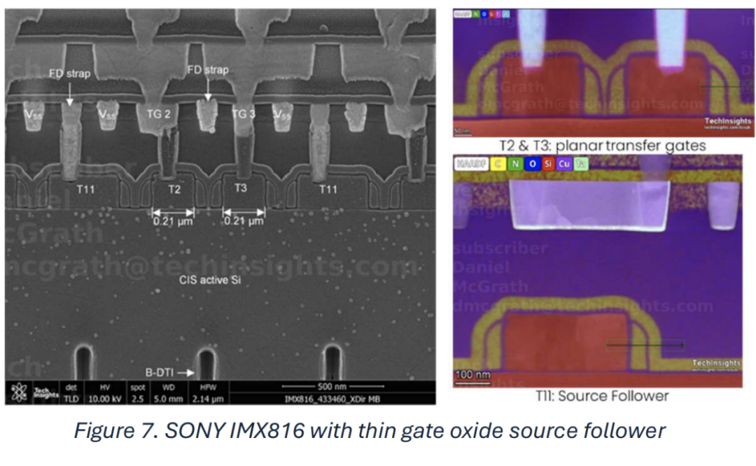
One characteristic of smartphone pixels is the use of dual gate oxide layers, with thinner source follower transistors and thicker control field-effect transistors (FETs) (Figure 7).
Given that image sensors are both integrated circuits and transducers, novel structures and material choices are required to provide photonic performance. This includes forming back structures to reduce dark signal generation and enhance optical response. While there seems to be a consensus on using AlO/ZrO as layers deposited on the back of silicon to suppress charge generation, manufacturers are choosing between TaO and HfO for the next layer (Figure 8).
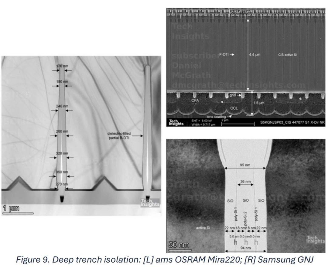
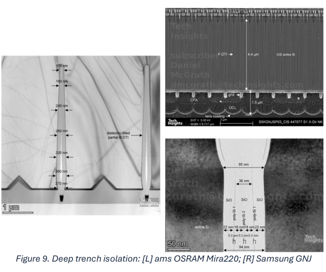
The uniqueness of this photodiode lies in its deep trench isolation, which reduces light loss and prevents optical carrier crosstalk between pixels. The etching depth of this photodiode ranges from 10:1 to 40:1, filled with conformal material layers with thicknesses from 10nm to over 100nm (Figure 9). The materials used include SiO, polycrystalline silicon, W, AlO, TaO, and TiN.
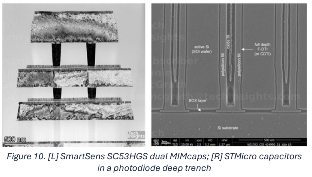
The momentum of pixel development has shifted from shrinking 4T pixels or their shared versions to adding more functionalities to pixels. Improved capacitors are key to increasing high dynamic range and global shutter capabilities. Available capacitors include MOS capacitors, parasitic FET capacitors, staggered capacitors, and capacitors formed by connecting adjacent row elements. Using nanodielectrics and placing MIM caps in the interconnect layer can achieve small pixels with global voltage domains (Figure 2).
Due to space constraints, pixels will mix various types of capacitors, but SmartSens has adopted stacked MIM caps as an alternative (Figure 10L). STMicro has formed capacitors in pixels located either externally or internally within the deep trench isolation of the photodiode layer (Figure 10R).
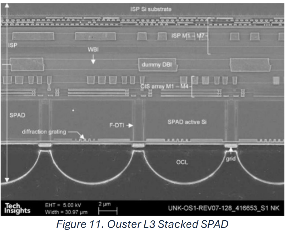
The emergence of wafer-to-wafer interconnect technology for small pixel pitch has enabled SPAD sensors to achieve a 100% fill factor, as pixel circuits can now be placed behind the photodiode (Figure 11).
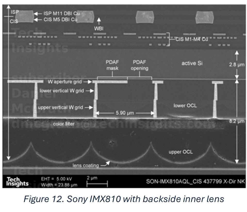
In high-end MILC camera applications, innovation or a re-examination of past concepts is still evident. Sony’s combination of back-illuminated light pipes with built-in lenses demonstrates this (Figure 12).
Enhanced image sensor-specific processes have enabled non-photographic imaging. Eye-tracking in augmented reality headsets requires imaging beyond the visible spectrum, thus image sensors have utilized all technologies in the near-infrared (NIR): 6.4µm photodiode silicon wafers; deep trench isolation; back-illuminated pyramid arrays (Figure 13). This component benefits from the small size brought by stacking technology.
The first multispectral smartphone camera features a 3×3 color filter array, with a color pixel in each array, created without the need for color filters or microlenses (Figure 14). This application seems suitable for visible light wavelengths to provide color correction information.
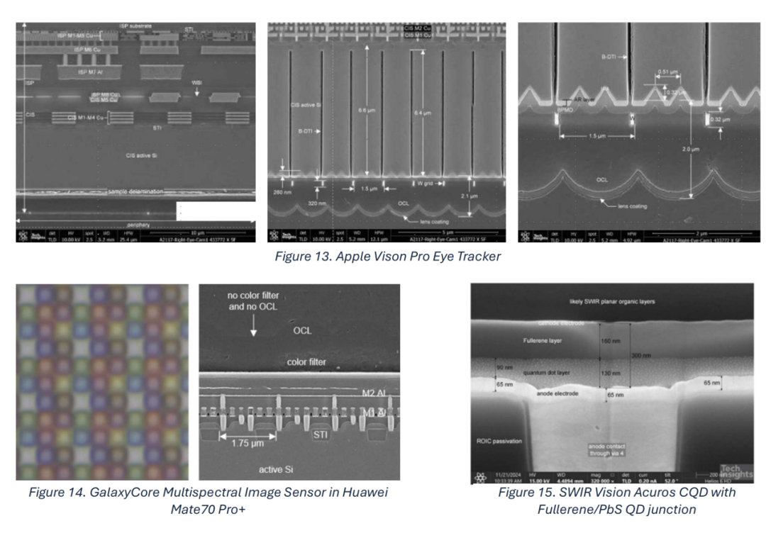
Imaging in the short-wave infrared (SWIR) band requires innovation for commercial applications, as silicon does not absorb wavelengths above 1.0µm. The challenge lies in manufacturability and environmental issues related to toxic substances. An innovative approach to address the former is to construct a transparent fullerene n-p junction and absorb PbS quantum dots on silicon readout integrated circuits (Figure 15).
Even as the pixel sizes for applications seem stable, image sensor products continue to benefit from process improvements, underscoring the value of ongoing technological development. Stacking with pixel-level interconnects can achieve multilayer stacking, presenting an opportunity, while the shift from driving smaller pixels to manufacturing pixels with additional functionalities opens up possibilities. Currently, image sensor technology has reached astonishingly low costs per pixel, so our industry is no longer limited to a single dominant product but has a broad development prospect.
Click here 👆 to follow for more original content
*Disclaimer: The content of this article reflects the author’s personal views, and Semiconductor Chip News reproduces it solely to convey a different perspective, not representing Semiconductor Chip News’s endorsement or support of this viewpoint. If there are any objections, please feel free to contact us.
Recommended Reading
100 trillion, invested in semiconductors
Chip giants, market value plummets
Jensen Huang: HBM is a technological miracle
Jim Keller: RISC-V will definitely prevail
The 10 highest-valued chip companies globally

If you like our content, please click“Looking” and share it with your friends~