Nash Bell
President of BEST, Inc.

Since the late 1990s, Ball Grid Array (BGA) packaging has become the preferred packaging method for electronic devices. Compared to high-density ultra-fine pitch Quad Flat Packs (QFP), BGA packaging can significantly reduce the footprint required on the PCB by approximately 50%.
Integrating standard BGA and its stacked counterparts, known as Package-on-Package (PoP), can further enhance density, providing greater design flexibility for compact and efficient circuit designs in applications ranging from consumer electronics to automotive systems and medical devices. Despite these advantages, the complexity of BGA packaging presents challenges in the rework process, necessitating innovative approaches and thorough routine inspection methods to maintain performance and reliability.
Diving Deep into High-Growth Markets to Create Full-Stack Solutions
BGA rework involves the removal and replacement of BGA packages on PCBs due to defects, upgrades, and/or failures (Figure 1). This process is crucial for ensuring the integrity and functionality of electronic devices. Engineers can employ various technical methods, each with its unique advantages, which need to be carefully considered based on the specific application.
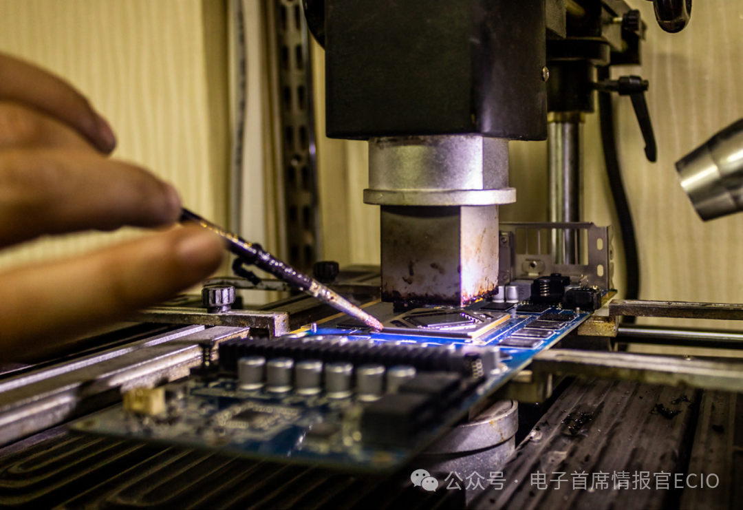
Figure 1: Hot air rework is a process that uses a stream of hot air to uniformly heat the BGA and PCB.
There are many methods available for removing and replacing BGA components. The specific method chosen depends on various factors, including available equipment, board density, and the skill level of the rework technician. These methods include:
1. Hot Air Rework: This method uses a stream of hot air to uniformly heat the BGA and PCB, melting the solder and then removing the package (Figure 1). While effective, this method requires careful control to prevent thermal damage to adjacent components.
2. Infrared (IR) Rework: This method uses an IR emitter aimed directly at the BGA, minimizing thermal impact on surrounding areas. Calibration is crucial for achieving uniform heating.
3. Vapor Phase Rework: This method involves placing the PCB in a chamber filled with vapor to provide uniform heating. While it offers excellent thermal management, it can be too costly for batch applications.
4. Laser Rework: This method uses a focused laser beam for precise heating, allowing selective reflow while minimizing damage to adjacent components. This technology requires significant investment in specialized equipment.
5. Precision Milling: This method is primarily used for removing components with bottom fill. It employs high-precision equipment to remove a layer of the BGA in one go. Although this method destroys the component, it allows for subsequent placement in the same location, reducing the risk of pad damage.
Equipment and Skill Requirements
Modern BGA rework requires complex equipment with precise placement capabilities, as well as skilled technicians to operate these systems effectively.
Modern BGA rework necessitates specialized equipment with precision placement capabilities, along with highly skilled technicians capable of operating these systems proficiently. Improper equipment operation or inexperienced technicians can lead to defects and rework failures. To address these issues, investing in advanced programmable rework systems with precise temperature control and calibration capabilities is essential, complemented by ongoing training programs to ensure technicians are adept at mastering evolving new technologies. Combining top-tier tools with continuous skill enhancement can improve the reliability, accuracy, and overall success rate of the BGA rework process. Selecting the right heat source, nozzle, and employing preheating techniques can ensure even heat application, reduce thermal stress, and minimize damage such as warping or pad lifting. Throughout the rework process, careful process planning and control are critical to maintaining the integrity of the components.

The above is an advertisement and is not related to the main content.
Typical BGA Rework Challenges
The inherent risks of BGA rework can jeopardize the quality and functionality of electronic components. The complexity of handling BGA components and the precision required for effective soldering increase the likelihood of misalignment, solder defects, and thermal damage. Issues such as PCB delamination, BGA package cracking, and damage to adjacent components can arise due to improper rework techniques or inadequate thermal management. Additionally, introducing contaminants during the rework process can compromise the integrity of solder joints. Below are six common challenges encountered during BGA rework:
1. Damage to Adjacent Components
When reworking a BGA, it is crucial to assess the surrounding components, especially those located nearby or on the opposite side of the PCB, as they may be affected by heat during the rework process. Sensitive components such as capacitors, crystals, and plastic parts are easily damaged by improper temperatures, making precise temperature control, targeted heating, and strategic cooling essential. Using physical barriers or thermal shields can help protect these vulnerable areas. Selecting the right heat source, nozzle, and employing preheating techniques can ensure even heat application, reduce thermal stress, and minimize damage such as warping or pad lifting.
2. Large BGAs
As large BGA packages measuring 125mm x 125mm become increasingly common, the limitations of existing systems (e.g., misalignment with split prism vision technology, insufficient power from bottom heaters) present significant rework challenges, leading to uneven heating and potential damage. Maintaining uniform temperature across a large surface is difficult due to airflow disturbances, and infrared systems often lack the appropriate spot size for achieving uniform heating. To overcome these challenges, technicians can employ custom support fixtures, use removable steel meshes, and optimize temperature profiles. These measures can enhance stability, improve soldering quality, and increase process reliability for large BGA rework under constrained systems.
3. Bottom-Filled BGAs
Bottom fill materials, typically made of epoxy or polymer, are used to protect BGAs. They often lead to displacement at the corners, resulting in defects such as mechanical stress and issues related to the coefficient of thermal expansion (CTE). While bottom fill is effective in protecting components, it can pose significant challenges during rework. Typically, hot air reflow methods are unsuitable as they can liquefy the bottom fill, hindering reliable solder joint formation.
Effective rework techniques include controlling the reflow to create a clear separation line, requiring precise temperature and force to avoid damage. Another approach is to use specialized softeners to weaken the adhesion of the bottom fill, allowing for safer removal of components and minimizing the risk to the PCB. When retaining old components is not feasible, cold milling provides an alternative by precisely removing a thin layer of the component in one go, leaving minimal residual solder at the pad location, which can be easily cleaned for subsequent BGA placement. Cold milling requires specialized equipment and skilled operators to ensure reliable results.
4. Component and PCB Warping
Warping occurs when components experience rapid temperature changes, with factors such as heating rate, humidity, and component size affecting the degree of warping. It often leads to displacement at the corners, resulting in defects such as opens or bridging. To minimize warping during rework or assembly, strategies include using custom fixtures or clamps to hold components flat, localized heating to relieve internal stresses, thermal cycling to gradually release stress, and employing supportive cover materials. Adhering to industry guidelines such as J-STD-033 and JEDEC for moisture control also helps reduce the risk of warping. Combining mechanical, thermal, and procedural methods can ensure better alignment, connectivity, and overall reliability.
5. Mirrored BGAs
Mirrored BGAs—placing BGAs back-to-back on opposite sides of a double-sided PCB—pose rework challenges due to increased density and the risk of damaging bottom components. Traditional preheating methods expose the bottom BGA to prolonged high temperatures, risking warping, solder defects, and solder joint failures. To address this issue, localized heating techniques with precise temperature control, such as infrared or hot air rework, combined with thermal shields like aluminum foil or pads, can protect components on the opposite side. Using low-temperature solder and closely monitoring temperature profiles can further reduce risks, ensuring effective rework while maintaining component integrity.
6. Stacked Packages
Stacked packages (Package-on-Package, PoP) involve stacking BGAs, with logic or CPU modules at the bottom and memory on top, achieving a compact, high-density design ideal for portable devices (Figure 2). The proximity of stacked packages, fine pitches, and thin profiles increases the risk of warping, delamination, misalignment, and solder defects, making PoP BGA rework challenging. Successful rework requires precise temperature control, localized heating, custom fixtures, and skilled technicians. Thorough pre- and post-rework inspection, controlled ramp rates, and real-time monitoring help prevent damage and ensure component integrity. Implementing these strategies enables manufacturers to tackle the complexities of PoP rework while maintaining reliability and quality in space-constrained electronic components.
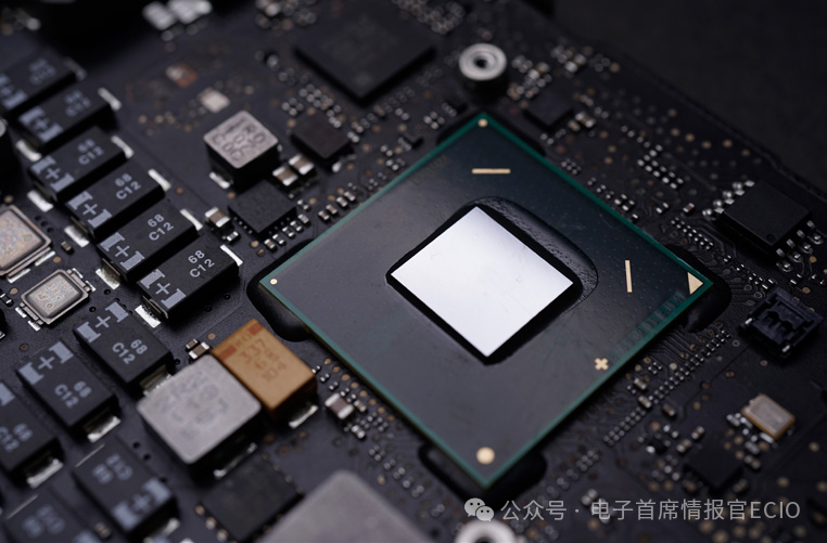
Figure 2: PoP involves stacking BGAs, with logic or CPU modules at the bottom and memory on top, achieving a compact, high-density design ideal for portable devices.
BGA Reballing
BGA reballing is a critical step in BGA rework, allowing for the reuse of components, repurposing of parts, or addressing solderability issues such as oxidation or solder ball damage. The specific process involves removing and replacing the original solder balls using various methods. Manually removing solder balls with solder wick is cost-effective but requires careful control to avoid damaging pads; whereas using a robot with hot solder paste to remove solder balls offers higher consistency and reduces the risk of pad scratching, although high temperatures may cause pads to lift. After removing the original solder balls, technicians use flux and specialized fixtures, solder masks, preforms, or advanced laser systems to place new solder balls. Each method balances factors such as cost, precision, and complexity. Post-reballing inspection is crucial for verifying correct solder ball placement, volume, coplanarity, and detecting defects such as shorts or foreign objects. A reliable reballing process is fundamental to achieving high-quality, defect-free BGA rework, especially when dealing with fine pitch or high-density assemblies.
BGA Rework Inspection
Effective inspection of BGA solder joints after rework is critical for ensuring connection reliability and the overall performance of electronic devices. Different methods provide varying technologies for assessing solder joint quality and potential issues, with each method suitable for specific applications. Typical inspection methods after BGA rework include visual inspection and X-ray inspection.
Visual Inspection
Visual inspection is a key first step in assessing solder joint quality, and conducting these inspections according to IPC-A-610 “Acceptability of Electronic Assemblies” is essential for ensuring compliance and reliability. Technicians often use magnifying tools such as microscopes or borescopes to carefully evaluate solder joints, alignment, and any visible defects. Key considerations for effective inspection include selecting the appropriate magnification, ensuring adequate lighting, and maintaining a controlled environment. Inspectors should check for common defects such as missing solder balls, solder ball size, solder bridging, and poor wetting, as these factors can affect the performance and longevity of solder joints. Implementing thorough visual inspections is crucial for achieving high-quality rework results.
X-ray Imaging
X-ray inspection is an important non-destructive testing technique used to assess the internal structure of solder joints, particularly those beneath BGAs, capable of detecting hidden defects such as shorts, opens, and pillow effect issues (Figure 3). To maximize efficiency, it is important to capture images from multiple angles, use appropriate magnification, and regularly calibrate the system to ensure accurate imaging. Additionally, comprehensive training for technicians in image analysis is crucial for accurately identifying defects such as voids or solder bridging.
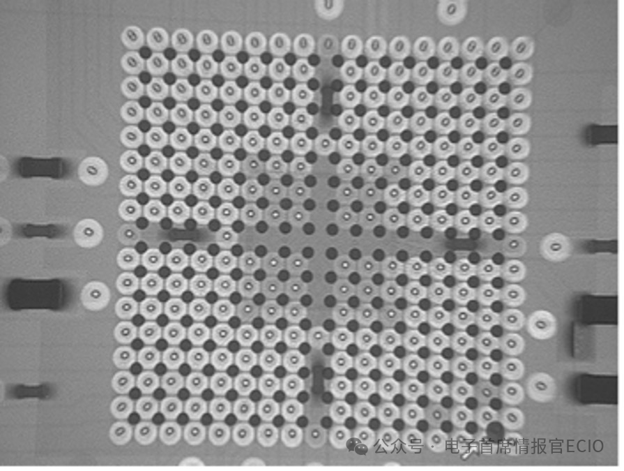
Figure 3: X-ray can detect hidden defects.
Proper calibration and skilled interpretation can significantly enhance defect detection, ensuring higher quality, reliability, and improving the overall assurance of electronic components.
Dye Pull Testing
Although dye pull testing is destructive, it is a valuable method for assessing solder joint quality, particularly after BGA rework. The process involves applying dye to the solder joint to reveal cracks, voids, or insufficient coverage, followed by carefully pulling the BGA package from the PCB to visually inspect the interface for defects. While highly effective for failure analysis and critical quality checks, it permanently damages the components and PCB. Proper procedures, including uniform dye application and controlled pulling force, along with trained technicians for skilled interpretation of results, are crucial for accurate outcomes. This method helps identify hidden defects that may affect long-term reliability, supporting higher quality assurance for electronic components.
Conclusion
Since the late 1990s, BGA packaging has become the preferred method for electronic device packaging, achieving significant space savings and high-density integration for modern applications.
Despite the advantages of BGA, its rework presents many challenges, including precise temperature control, handling bottom fill or large packages, warping, and the complexities of stacked packaging (PoP). Effective rework involves a range of techniques, from hot air, infrared, vapor phase to laser reflow, each generally suited for specific situations, requiring advanced equipment and skilled technicians.
Key processes such as BGA reballing, inspection (visual, X-ray, dye, and pull), and troubleshooting are essential for ensuring reliable, defect-free connections. Addressing inherent risks such as damage to adjacent devices, warping, and solder joint defects requires meticulous process planning, appropriate tools, and stringent quality checks. Ultimately, a combination of innovative technologies, ongoing operator training, and comprehensive inspection standards can ensure high-quality, reliable BGA rework, supporting the ongoing miniaturization and complexity of modern electronic systems.
END







The above is a partner of the Chief Electronics Officer (partially)
Order does not imply priority.