In FPGA design, clock management is the cornerstone for the stable operation of the entire system. Xilinx’s Clocking Wizard IP Core serves as a core tool for clock management, significantly simplifying complex clock designs. This article will guide you from basic usage to advanced applications, allowing you to fully master this powerful tool.
1. What is Clocking Wizard?
The Clocking Wizard is an IP core in the Xilinx Vivado design suite, used to automate and simplify clock management in FPGAs. It provides a graphical interface to configure MMCM (Mixed-Mode Clock Manager) and PLL (Phase-Locked Loop), enabling developers to generate stable and precise clock signals without needing to deeply understand the underlying complex clock architecture.
Core Value:
-
Graphical and automated design of complex clock management
-
Reduces design difficulty and risk of errors
-
Optimizes clock network performance and resource usage
2. Basic Usage
2.1 Invoking Clocking Wizard in Vivado
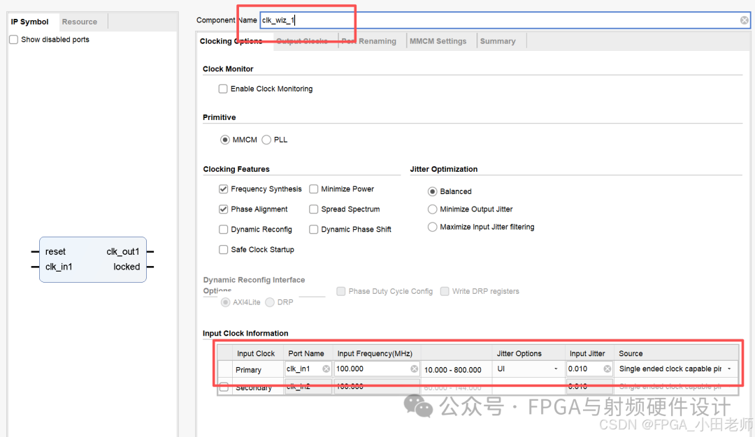
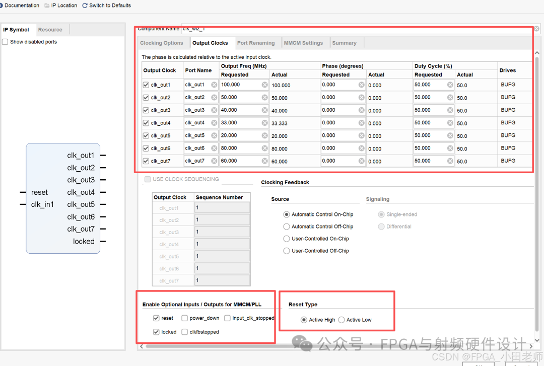
The typical usage is to open it and keep the defaults, providing an input clock and an output clock, which can generate one or more clocks with different frequencies or phases for use in various modules of your project. It also features clock de-jittering and phase adjustment, making it essential for almost every FPGA project.
2.2 IP Instantiation
// Generated instantiation template
clk_wiz_1 instance_name (
  .clk_out1(clk_100m),     // Output clock 100MHz
  .clk_out2(clk_50m),     // Output clock 50MHz
  ......
  .reset(reset_i),         // Asynchronous reset
  .locked(locked_o),       // Clock locked signal - very important!
  .clk_in1(clk_100m)      // Input clock 100MHz
);
3. Resource Consumption: Understanding Costs
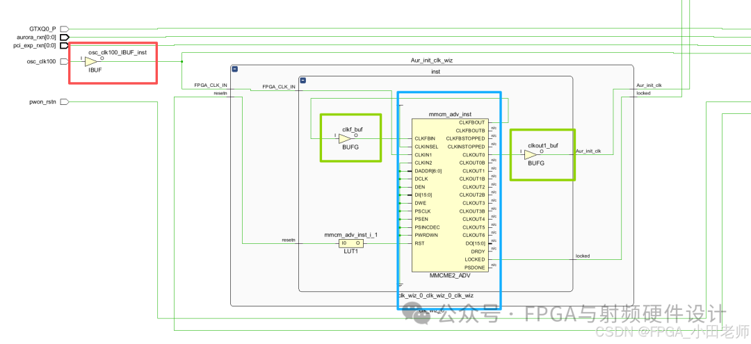
Its internal logic is shown in the figure below, where the external clk is sent into the IP core through IBUFG, and then through BUFG to MMCM/PLL. The output clock then passes through BUFG to become the final clock signal we obtain. This illustrates its resource consumption (Note: This diagram shows only one output clock; if there are 7 outputs, there will be 7 output paths. This needs to be compiled to see, so I found an existing one to show everyone the internal structure).
 If we generate 7 clocks from 1 clk_in, the consumption will be 8 BUFGs. When BUFG resources are tight, we can balance resources by selecting the output clock’s resource attributes, such as using BUFGCE, etc.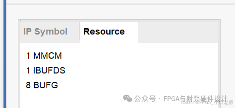
CMT – Clock Management Tile
-
Each CMT contains 1 MMCM + 1 PLL
-
Key Understanding: Using MMCM or PLL will consume the entire CMT
-
Example for XC7A100T: 6 CMTs → up to 6 MMCMs or 6 PLLs
BUFG – Global Clock Buffer
-
Each clock input/output typically requires 1 BUFG
-
Example: 1 input + 7 outputs = 8 BUFGs
-
XC7A100T has 32 BUFGs, requiring careful planning
4. MMCM vs PLL: How to Choose?
[Primitive] defaults to MMCM But what are the differences between MMCM and PLL?
Both MMCM and PLL will consume one CMT resource
Advantages of MMCM:
- Supports a wider clock range compared to PLL, supports fractional division/multiplication (PLL only supports integer)
- MMCM supports more output clocks; for example, with xc7a100t, one MMCM can output 7 clocks, while one PLL can only output 2 clocks.
Advantages of PLL:
- Lower power consumption compared to MMCM, making it advantageous in power-sensitive scenarios.
 5. Detailed Explanation of 10 Advanced Options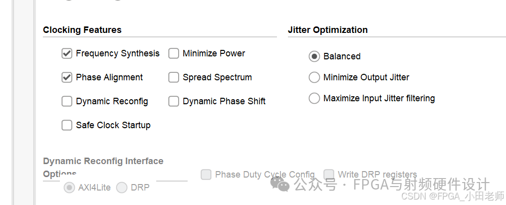
🎯 Frequency Synthesis
Function: Allows output clocks to have different frequenciesScenario: Any situation requiring clock frequency conversion
📡 Spread Spectrum
Function: Reduces electromagnetic interference (EMI)Limitation: Mutually exclusive with dynamic reconfigurationScenario: Products requiring EMC certification
⚡ Phase Alignment
Function: Locks the output clock phase to the reference clockCost: Occupies additional clock routingScenario: Strictly synchronized systems with multiple clock domains
🔋 Minimize Power
Function: Optimizes power consumption, potentially sacrificing accuracyScenario: Battery-powered devices, low-power applications
🎚️ Dynamic Phase Shift
Function: Dynamically adjusts clock phase at runtimeScenario: DDR interface debugging, high-speed serial communication
🔄 Dynamic Reconfiguration
Function: Reconfigures clock parameters after the device is runningInterface: AXI4-Lite or DRPScenario: DVFS, multi-mode communication systems
⚖️ Balanced
Function: Automatically optimizes jitter performanceScenario: Most general applications, default choice
🎵 Minimize Output Jitter
Function: Optimizes output clock qualityCost: Increases power consumptionScenario: High-speed ADC/DAC sampling clocks
🛡️ Maximize Input Jitter Filtering
Function: Enhances input clock jitter toleranceScenario: When the quality of the input clock source is poor
🚀 Safe Clock Startup
Function: Ensures the clock is output only after stabilization, supports startup sequencesScenario: Multi-module sequential startup systems
6. Practical Tips and Best Practices
Must Handle Locked Signal
// Incorrect: Directly using output clock
always @(posedge clk_out1) begin  // May start working before the clock is stable
end
// Correct: Use locked signal as reset condition
always @(posedge clk_out1) begin  sys_reset_n <= locked_o;
end
Conclusion
The Clocking Wizard is an indispensable tool in FPGA design. Proper usage requires:
-
Understanding Architecture: Mastering concepts like CMT, BUFG, etc.
-
Wise Choices: Making trade-offs between MMCM and PLL based on requirements
-
Utilizing Options: Reasonably configuring the 10 advanced options to optimize performance
-
Following Best Practices: Correctly handling the locked signal and planning resources
With the guidance from this article, you should be able to confidently use the Clocking Wizard in your projects to build stable and reliable clock systems. Remember, good clock design is half the success of an FPGA project!