Click the blue text to follow us


From a single chip to mass production, tape-out determines whether the chip design can be utilized. Each successful tape-out signifies a successful chip design. Since the beginning of this year, many domestic companies have announced successful tape-outs, which undoubtedly demonstrate significant progress in domestic chip development.
In the domestic GPU sector, Muxi announced the tape-out of its first high-performance general-purpose GPU chip, utilizing a 7nm process, expected to enter mass production in 2023; Jingjia Micro announced that its second GPU in the JM9 series has completed the tape-out and packaging stages; Xiangdi’s Tianjunjun No. 1 GPU entered tape-out in June this year.
In the automotive chip sector, Zhongying Electronics is developing automotive-grade MCUs, which have successfully completed tape-out and are in the verification phase; Guoxin Technology’s automotive domain controller chip CCFC2016B has completed tape-out; Loongson Technology stated during an institutional survey that it has developed a highly reliable automotive MCU chip for control, with the first chip already tape-out.
In the SoC chip sector, Xinyuan Technology has achieved a successful tape-out of a 5nm system-on-chip (SoC) in one go, with multiple 5nm one-stop service projects currently underway; Kuaishou has launched its self-developed SL200 SoC chip, which has successfully completed tape-out and is undergoing online testing.
With a continuous stream of tape-out news, domestic chip design companies are consistently breaking through the “tape-out” barrier.
 01
01
Tape-Out Determines Success or Failure
The importance of tape-out lies in its ability to verify whether the chip design is successful. Tape-out is a critical step in chip manufacturing, where the finalized design is handed over to the chip manufacturing plant to produce a few or several sample chips to test whether the designed chip can function or if further optimization is needed. If a chip that meets the requirements can be produced, then mass production can commence.
The risks associated with tape-out are extremely high. Historically, Xiaomi’s Pinecone Electronics suffered significant losses due to five consecutive tape-out failures of the Surge S2 series chips. For companies, a failed tape-out means that both time and financial resources are wasted, and the outcome of the next tape-out remains uncertain. Delaying the product launch in today’s volatile market can be fatal for a company.
There are many steps in the chip design process, and a mistake in any one step can lead to a tape-out failure. A chip design company representative summarized the reasons for tape-out failures:
First, the wrong version of the design is used, especially if the wrong ROM version is selected, rendering the chip essentially useless; second, there are some bugs that cannot be bypassed by software, such as when the chip cannot exit low-power mode after entering it during power management; in such cases, the chip may light up but cannot be used, which is a major error; third, for chips with very high security requirements, if there are hardware security vulnerabilities that software cannot circumvent, the tape-out is also considered a failure; fourth, even if the chip meets functional requirements, if it is an IoT chip with low power consumption requirements, excessive power consumption would also be deemed a tape-out failure.
Overall, tape-out failures can be determined not only by the hardware being unable to light up but also by failing to meet power consumption, circuit, and functional requirements.
Last year, when Horizon released the Journey 5 chip, its founder Yu Kai proudly announced: “The Journey 5 chip successfully completed tape-out in one go. We originally prepared for 150 hours of testing, but all passed in just 15 hours.” Horizon’s success in one go indicates the strength of its research team. However, in the chip manufacturing process, cases of successful tape-out in one go are very rare; most design companies need to undergo multiple tape-outs.
Some analog chip companies, even with a complete team and clear ideas, took 8 years and went through 18 tape-outs to finally complete the verification of sensor analog computing IP, creating the ideal “ultra-low power, ultra-close sensing” chip.
02
Strong Support for Tape-Out Policies
This critical step is extremely costly. Some smaller design companies have announced their closure after multiple tape-out failures. An engineer stated: “My previous company was ruined by tape-out failures.”
Many factors influence the successful manufacturing of a chip, including the type of process used, the size of the wafer, and the chip EDA design. Each choice in these steps affects the tape-out success rate and cost. The cost of tape-out mainly depends on the semiconductor process, that is, the chip manufacturing process. With the upgrade of semiconductor processes, both chip design and tape-out costs are expected to increase exponentially.
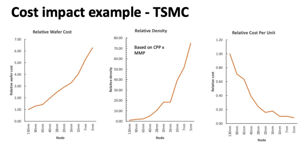
Example of TSMC Cost Impact
Describing tape-out costs as “in the millions or even hundreds of millions” is not an exaggeration. According to statistics, the cheapest ASIC tape-out costs around hundreds of thousands per attempt, with the cost for 180nm tape-out being approximately 500,000 yuan, 55nm costing around 2 million yuan, and 16nm skyrocketing to 30-50 million yuan, while 7nm costs at least over 100 million yuan.
An engineer who has worked at SMIC analyzed the tape-out process and costs. The cost of a chip is divided into two parts: the cost of the mask and the cost of the wafer. In simple terms, cost = mask fabrication cost + N * single wafer cost.
After the chip design is completed, complex image files are produced, generally consisting of 30-50 layers, which need to be made into masks at a mask factory. The higher the process node, the more expensive the tape-out price, as higher processes require more masks. For example, a 14nm process requires 60 masks, while 7nm requires over a hundred masks.
Due to the varying precision of each layer of the mask, there are some differences in mask prices, but overall, a 40nm mask costs about 300,000 to 500,000 USD, and the wafer cost per piece is around 1500-2000 USD. Therefore, for design companies producing a few to dozens of chips, the main cost is for the masks.
Since the number of chips produced during tape-out is small, the mask cost of 300,000 to 500,000 USD is spread across each chip, making the cost extremely high; however, when mass production occurs, the same mask cost is spread across hundreds of thousands of chips, significantly reducing the relative cost.
Tape-out is indeed a critical life-and-death issue for design companies, which is why the domestic government has consistently introduced corresponding policies to support tape-out. In fact, as early as 2000, the Ministry of Finance and the State Administration of Taxation notified the General Administration of Customs that integrated circuit products designed domestically and possessing independent intellectual property rights, due to the inability to produce domestically, would have the portion of the import value-added tax exceeding 6% refunded immediately when tape-out and processing are done abroad.
This year, various provinces’ 14th Five-Year Plans have also shown special support for tape-out.
Shanghai is providing favorable tape-out services for eligible design companies to promote the application of integrated circuit production lines with a line width of less than 28nm (inclusive), with related tape-out fees counted as new project investments, providing 30% support for tape-out fees, with the support amount generally not exceeding 100 million yuan.
Beijing rewards companies conducting the first round of tape-out (full mask) for engineering products with 30% of the product tape-out costs, with a maximum annual reward of no more than 10 million yuan per company; for engineering products’ first round of tape-out (full mask) conducted in Beijing, a reward of 50% of the product tape-out costs is given, with a maximum annual reward of no more than 20 million yuan per company.
Hengqin provides an annual maximum tape-out subsidy of 30 million yuan for companies or research institutions conducting the first round of full mask tape-out before mass production of engineering products.
From the perspective of tape-out support, cities like Shanghai, Suzhou, Hangzhou, Hefei, Zhuhai, and Guangzhou offer substantial subsidies. Among them, Shanghai’s tape-out subsidy can reach up to 100 million yuan, while Zhuhai offers an annual maximum subsidy of 30 million yuan.
03
MPW and Full Mask Modes
To address the high tape-out costs, the industry has evolved two tape-out methods: Full Mask and MPW.
MPW (Multi Project Wafer) is a tape-out method adopted by many small design companies. In simple terms, MPW involves placing multiple integrated circuit designs with the same process on the same wafer for tape-out, sharing the tape-out costs based on area.
Industry insiders state: “The benefit of Share Mask is cost savings, but since you have to wait for others’ data to be ready, it requires more time. Generally, large companies will use their own set of masks, as 300,000 to 500,000 is not too high for them; small companies prefer Share Mask since 300,000 to 500,000 is not easy to come by.”
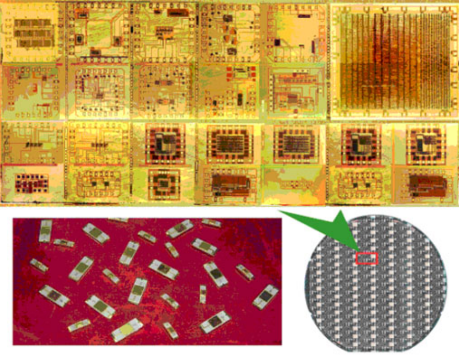
The following image is an example of their MPW service, where the circular area in the lower right is a complete 6-wafer, and the rectangular area marked with a box is the intermediate data obtained after stitching by the MPW processing service organization, with the small rectangles in the box representing different chips designed by different design companies. The upper half of the box is shown in an enlarged view. The lower left of the image shows the packaged integrated circuit chip. In actual processing, the stitched rectangle is treated as a (virtual) chip for tape-out manufacturing. According to the requirements of the integrated circuit processing line, a certain number of wafers (usually more than 5) must be produced in one processing run, so one MPW processing can provide enough samples for design companies.
Foundries will release the next year’s MPW schedule fixedly (mostly in Q4) each year, and companies will report their needs accordingly. Generally speaking, the more advanced the process, the higher the frequency of MPW arrangements; for more mature processes, there may be very few occurrences throughout the year.
Insiders from IC design companies reveal: “Under advanced processes (below 55nm), the process plant generally arranges the wafers in advance, dividing them into multiple areas labeled A, B, C, D, etc., and quoting prices. Each company can reserve one or more areas based on their situation, and they can further choose to place multiple test chips in their area (distinguished by logos).”
Some large wafer foundries will choose the Full Mask mode. Full Mask means that all masks used in the entire wafer manufacturing process are dedicated to a specific chip, which clearly incurs very high costs. However, this method can shorten the time from tape-out to subsequent mass production by about three months. In the race against the market, an earlier finished product naturally represents a larger market share.
At the same time, some domestic design companies that directly adopt Full Mask also demonstrate absolute confidence in their development capabilities.
Previous Highlights
 1. Overview of Domestic IP Companies 2. Overview of Domestic EDA Companies 3. Practical | Linux Operation Demonstration 4. Differences Between “Formal” and “Non-Formal” Engineers 5. This Summer, the Mee Talent Cloud Training Base Officially Opened in Zhangjiang! 6. Major Chip Design Companies (Fabless) in Beijing, Shanghai, Shenzhen, Hangzhou, Chengdu, Wuhan, Hefei, Chongqing 7. Summary of Daily Questions 1-83, How Many Classic IC Question Types Have You Seen?

E Course Network (www.eecourse.com) is a professional integrated circuit education platform under Moore Elite, dedicated to cultivating high-quality integrated circuit professionals in the semiconductor industry. The platform is oriented towards the job demands of integrated circuit companies, providing a training platform that fits the corporate environment, and quickly training students to meet corporate needs through online and offline training methods.
E Course Network has a mature training platform, a complete curriculum system, and a strong faculty, planning 168 high-quality courses in China’s semiconductor field, covering the entire integrated circuit industry chain, and has four offline training bases. To date, it has deeply trained a total of 15,367 people, directly supplying 4,476 professional talents to the industry. It has established deep cooperative relationships with 143 universities and has held 240 special IC training sessions for enterprises.