Introduction to Senhui: Suzhou Senhui Semiconductor, supported by a strong research and technical team, focuses on providing complete process solutions and wafer services for global compound semiconductor customers. The team members have deep experience in the semiconductor industry, with decades of rich capabilities in photolithography, thin film processes, epitaxy, bonding processes, as well as etching, wet processing, and polishing, showcasing mature technology and extensive process experience.
In the field of semiconductor packaging, hybrid bonding technology is sparking a new wave of transformation. This innovative process achieves “molecular-level” interconnections in chip stacking through the dual combination of metal and dielectric, opening up new possibilities for high-performance computing chips.
1. Technical Principles and Process Innovations
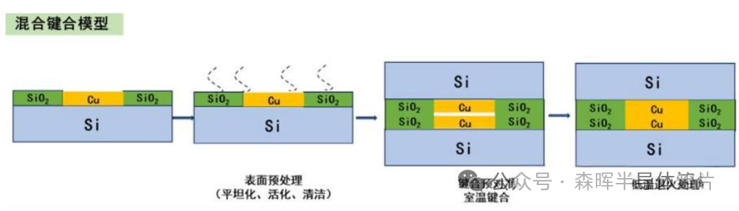
The core of hybrid bonding lies in the copper-dielectric composite structure (such as Cu/SiO₂, Cu/SiCN), which achieves atomic-level bonding of chips through a three-step precision process:
-
Ultra-precision Surface TreatmentUtilizing chemical mechanical polishing (CMP) to control the surface roughness of the wafer to within 0.5nm (dielectric layer) and 1nm (copper layer), combined with plasma activation treatment to form a hydrophilic surface.
-
Nano-level Precise AlignmentIn an ultra-clean environment with ISO Class 1 cleanliness, two wafers achieve sub-micron level (<1μm) positioning through an optical alignment system, with the dielectric layer forming an initial bond through chemical bridging.
-
Thermal Diffusion Reinforcement ProcessHigh-temperature annealing at 200-400℃ promotes the inter-diffusion of copper atoms, forming a permanent metal bond, with interface resistance reduced to 10⁻⁸Ω·cm² level.
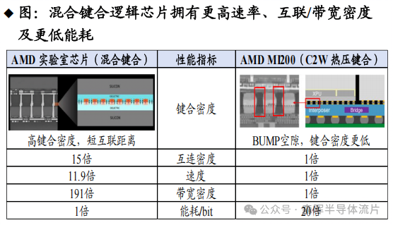
2. Performance Leap: Comprehensive Advantage Over Traditional Processes
Taking the AMD hybrid bonding chip and thermocompression bonding MI300 as an example:
- Interconnection density increased by 15 times, achieving 10⁶ connection points per unit area
- Signal transmission speed increased by 11.9 times, with latency reduced to 0.1ps/mm
- Energy efficiency optimized by 20 times, with power density only 1.5mW/mm²
- Bandwidth density surged by 191 times, reaching 5Tb/s/mm²
In HBM memory chip applications, it also demonstrates unique advantages:
- Thermal resistance reduced by 20%, with heat dissipation efficiency improved to 3W/m·K
- Signal integrity improved by 20%, with crosstalk suppression reaching -50dB
- Dynamic power consumption reduced by 17%, with energy efficiency ratio exceeding 85%
- TSV interconnection area reduced by 87%, with space utilization reaching 92%
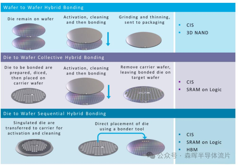
3. Comparison of Two Major Technical Routes
| Type | Applicable Scenarios | Advantages | Challenges |
|---|---|---|---|
| W2W Bonding | Small-sized chips | Yield >99.9%, low contamination risk | Cannot screen qualified chips |
| D2W Bonding | Large-sized chips | Supports pre-screening, mature industrialization | Cleanliness must reach ISO Class 0.5 |
4. Key Points of Technological Breakthroughs
-
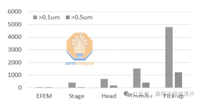
Ultra-clean Environment ControlMust maintain cleanliness of ≤10 particles of 0.1μm per cubic meter, equivalent to 1000 times the standard of an operating room.
-
Atomic-level Surface TreatmentUtilizing a dual-stage CMP process, the copper layer removal rate is precisely controlled at 100nm/min±5%.
-
Sub-micron Level Alignment SystemEmploying infrared alignment + machine vision technology, achieving precision of 0.8μm@3σ.
With the surge in demand for 3D packaging, the hybrid bonding market is expected to exceed $4.8 billion by 2025. This technology is reshaping chip architecture; what transformations do you think it will bring to AI chip development? Feel free to share your insights in the comments section.
For more information on gallium arsenide wafers, silicon carbide wafers, gallium nitride wafers, 4-inch wafers, 6-inch wafers, 8-inch wafers, and 12-inch wafers, please contact 15262626897 for detailed communication.