“Based on the XCKU040 development board, this article shares the functionality of data communication and processing between a host computer and FPGA via PCIe. Feel free to communicate; leave a message/private message to obtain the relevant source code.。”
FPGA PCIe is commonly used in applications such as data acquisition, communication, and acceleration.
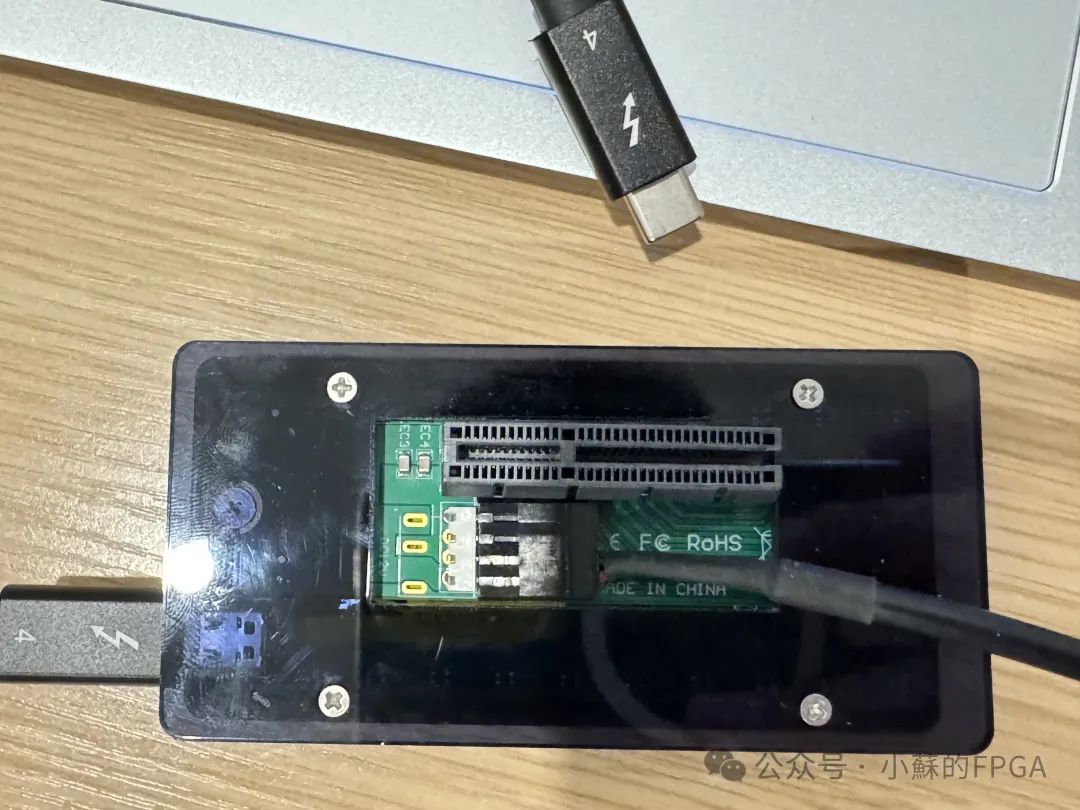
This article takes the Xilinx development board ku040 with PCIe 3.0 as an example, using a Thunderbolt to PCIe adapter board to achieve communication with the host computer.
01
—
PCIe Core IP
Using Vivado to call PCIe related hard IPs: there are three types for the transaction layer interface.
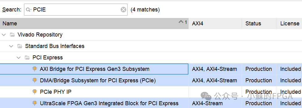
Integrated Block for PCI Express: This is the most basic PCIe IP, implementing the physical layer and data link layer of PCIe, providing users with AXI4-stream interface TLP packets. It has the smallest resource usage among the three types of IP, is flexible, but has the highest development difficulty. Using this IP requires a clear understanding of the PCIe protocol and TLP packets.
AXI Bridge for PCI Express: This encapsulates the above IP core, simplifying the design and providing an AXI M/S bridge, achieving AXI4 to stream functionality. When using this IP, users only need to receive and send PCIe data through the AXI4 interface without needing to encapsulate and parse TLP packets. Resource usage and development difficulty rank in the middle among the three types of IP.
DMA/Bridge Subsystem for PCI Express: This is XDMA, which not only completes the packaging and unpacking at the transaction layer but also adds DMA. It consumes the most resources but has the least development difficulty, allowing users who do not understand the PCIe bus protocol to develop PCIe application scenarios. XDMA is simple to use but has limitations:
1) Suitable for large-scale data transfer scenarios, not suitable for small data scenarios;
2) XDMA can only be used for PCIe endpoint devices.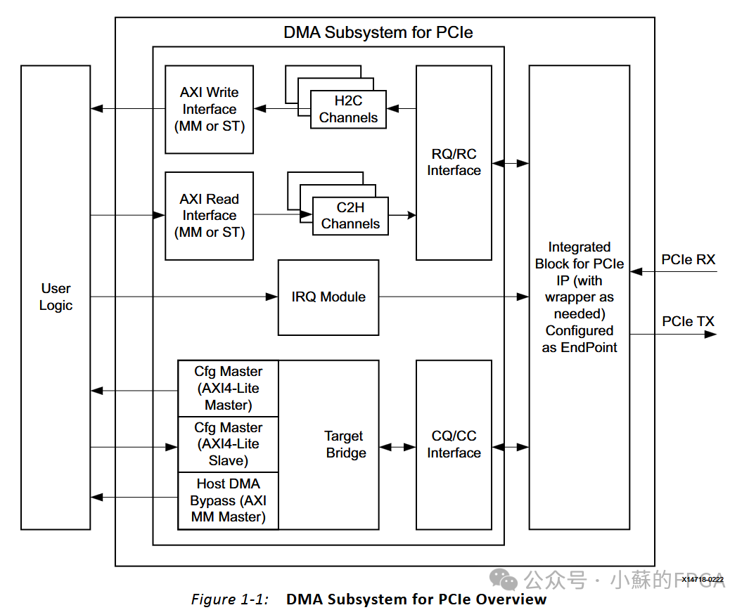
02
—
AXI Interface Protocol
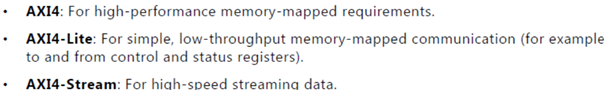
During the use of the PCIe core, the interface types provided to the user mainly include AXI-Stream, AXI-Lite, and AXI (AXI-Full).
XDMA’s AXI interface is mainly used for data interaction, suitable for large amounts of data based on address access (such as DDR); AXI-Lite is used for data interaction based on address access, such as registers, interrupts, etc.
AXI (Advanced eXtensible Interface) is a type of bus protocol proposed by ARM in the AMBA protocol, used for bus interconnection.
For more information on the AXI protocol, please refer to the Datasheet:
Independent read/write, out-of-order transmission (initiating multiple read/writes), out-of-order (ID)
Based on address: low-speed single address, high-speed burst/ out-of-order (DDR, BRAM)
Based on data stream: high-speed, large amount of unrestricted, no address
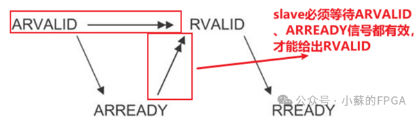
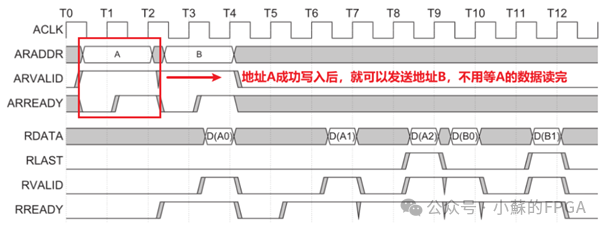
AXI achieves data interaction through valid and ready handshakes: for example, the interaction process of read address and read data channels.
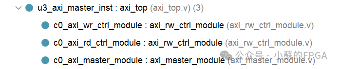
Based on this, an AXI master read/write interaction module was developed:
 Testing module development functions normally by calling AXI RAM: Calling RAM IP, selected as AXI interface:
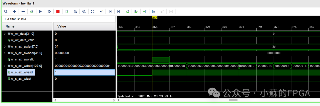
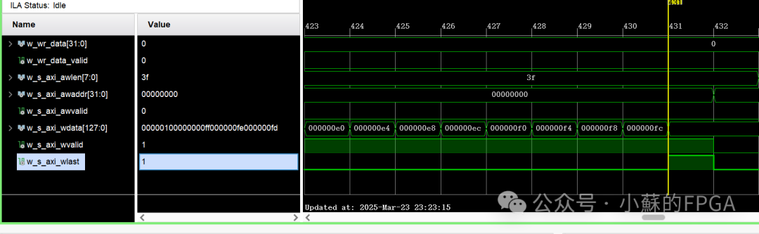
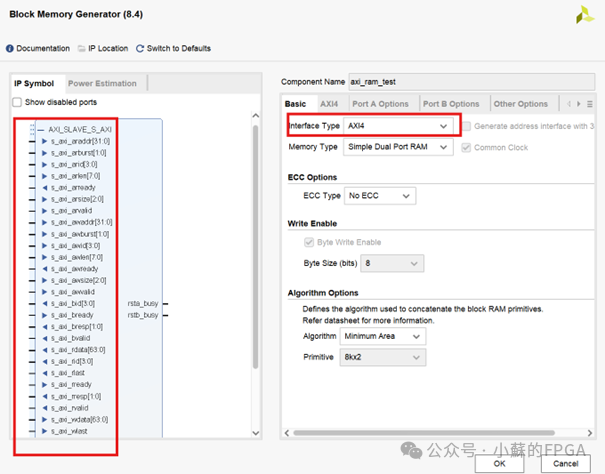 During the write process, AXI address, data, and response channel signals: each burst writes 1 data
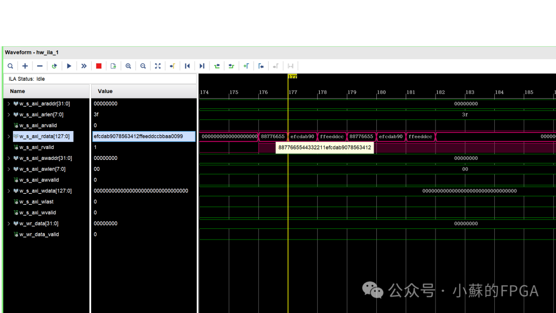
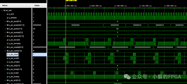 During the read process, AXI address and data channel signals: each burst reads 128 data
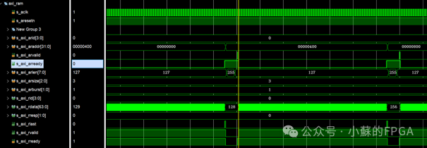
03
—
XDMA Core Configuration
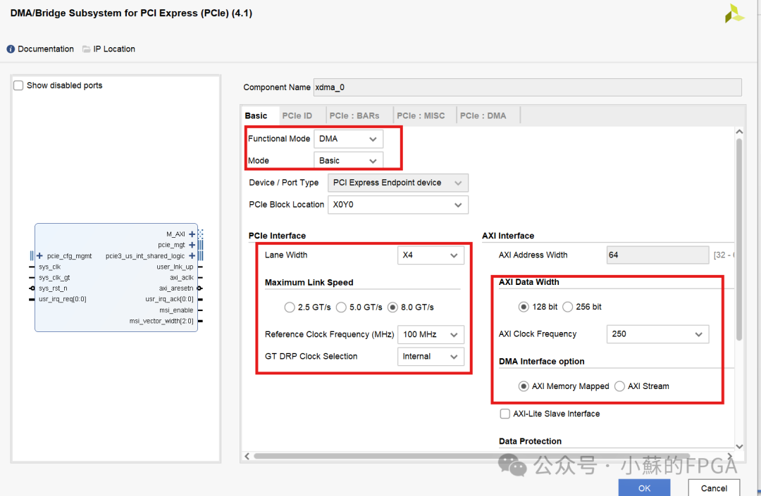
XDMA is a SG mode DMA core provided by Xilinx that can be used for PCIe 2.0 and PCIe 3.0. It can be configured with AXI4 interface or AXI4-Stream interface. If configured as AXI4 interface, it can easily connect to the AXI bus interconnection for data transfer with DDR.
Based on the hardware device PCIe 3.0 X4, select 4 lanes, 8GT/S, with the on-board GT clock at 100MHz, and select X0Y0 according to the PCIe schematic Quad position. This project involves data interaction between the host computer and DDR via PCIe, selecting AXI memory mapping, with a data width of 128 bits.
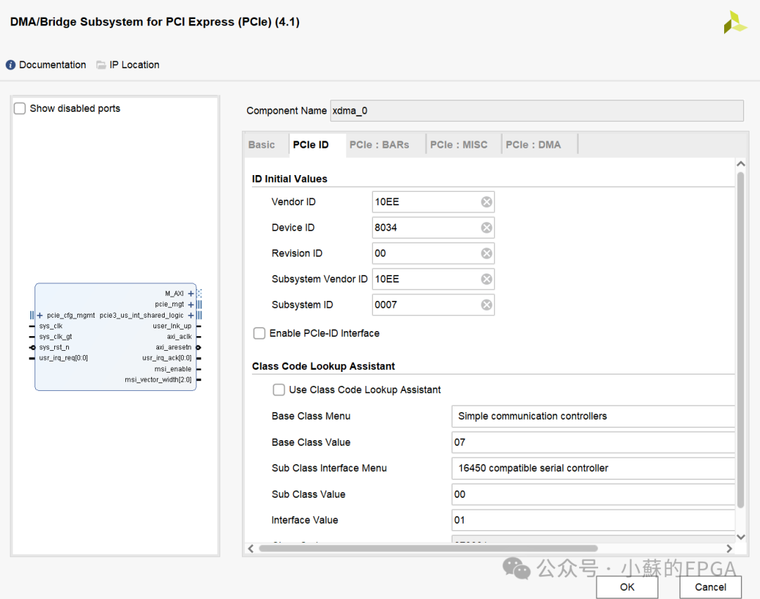
The PCIe ID option can be kept as default:
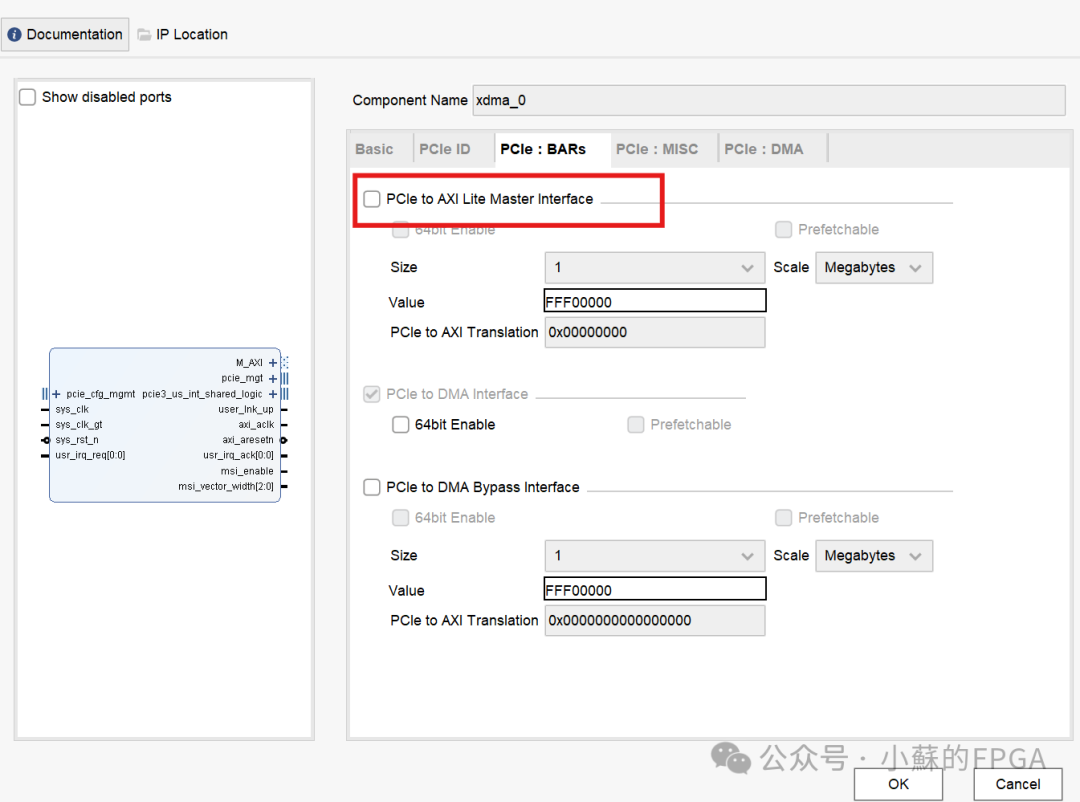
The PCIe BARS option: The AXI4-Lite Master interface can be used to implement the mapping from PCIe BAR addresses to AXI4-Lite register addresses, which can be used to read and write user logic registers, such as using BRAM or GPIO, etc. This test does not use the AXI-Lite interface.
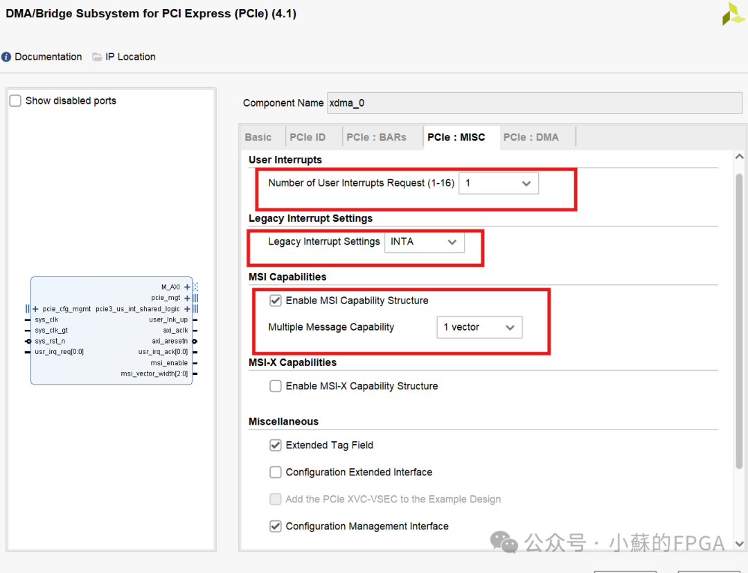
Setting the PCIe MISC interrupt options:
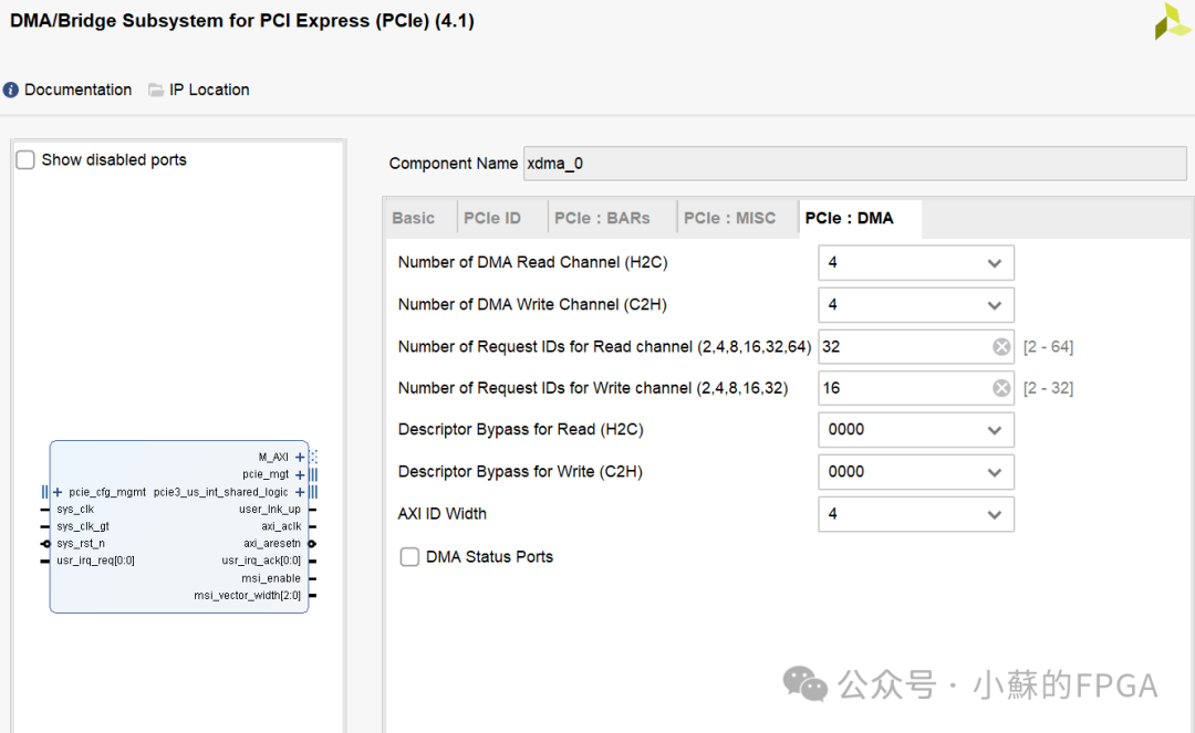
Setting the PCIe DMA read/write channel:
04
—
Project Setup
Add the XDMA IP core in Block Design and configure as mentioned above, add the DDR IP core and configure it as AXI interface, and automatically connect to add the reset module.
Disconnect the XDMA M_AXI to DDR_S_AXI connection, insert AXI_Interconnect (2 Master, 1 Slave); correspondingly modify its clk rst scope.
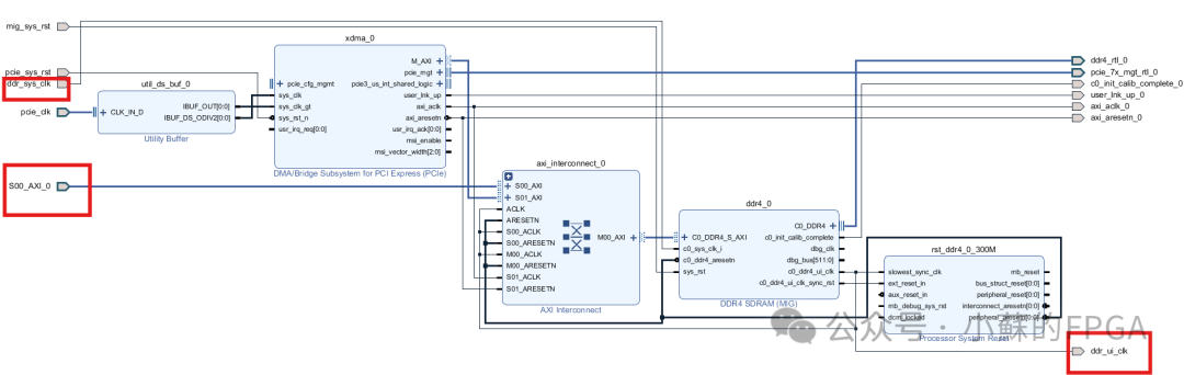
The user-side read/write DDR interface isS00_AXI_0.
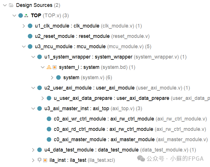
Code instantiation of each module: clock, reset, BD module.
Among them, the user_axi_module module converts the user interface of the data_test_module module into an AXI interface, combined with the above-coded axi master function axi_top module to achieve read/write functionality with DDR through S00_AXI_0.
05
—
Function Testing
Hardware device: PCIe to Thunderbolt card (PCIe X4 slot)
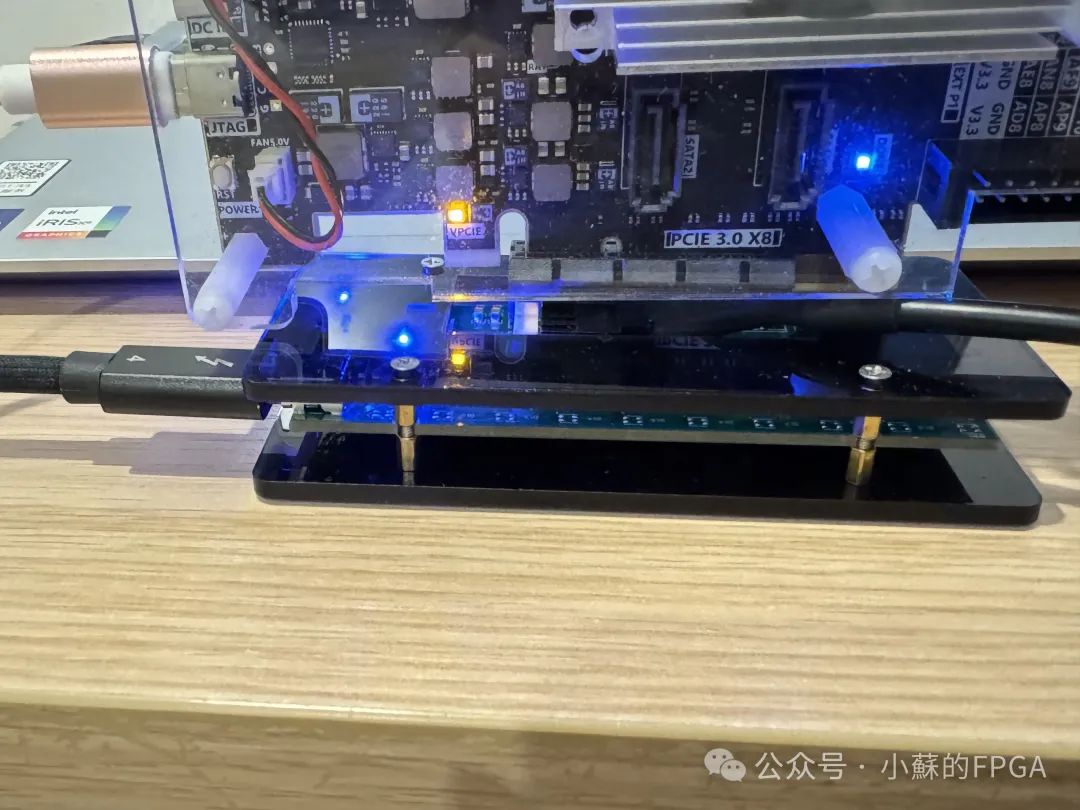
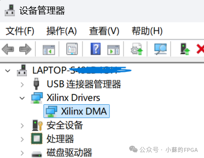
The host computer needs to install the PCIe driver for the first use, download the program to the board, and under normal circumstances:
 The test items are as follows:
- Read/write speed test
- Host write data and read data test
- Host write data, FPGA read data
- FPGA write data, host read data
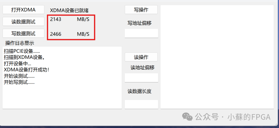
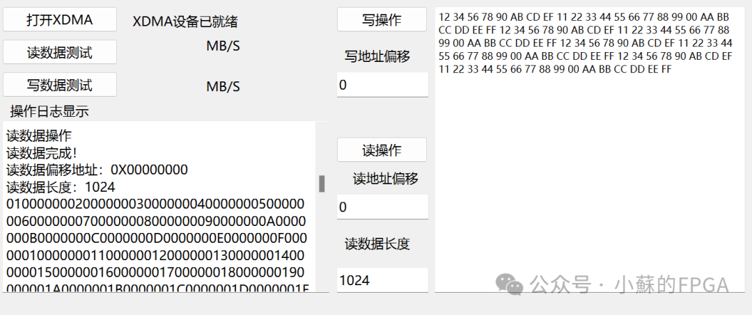
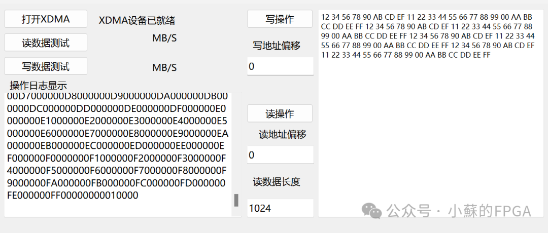
QT host testing interface for testing:
Device connection and read/write speed test: Device connection is normal, write data rate is about 2100MB/S, read data rate is about 2400MB/S. (PCIe 3.0 X4 theoretical bandwidth is about 4GB/S.)
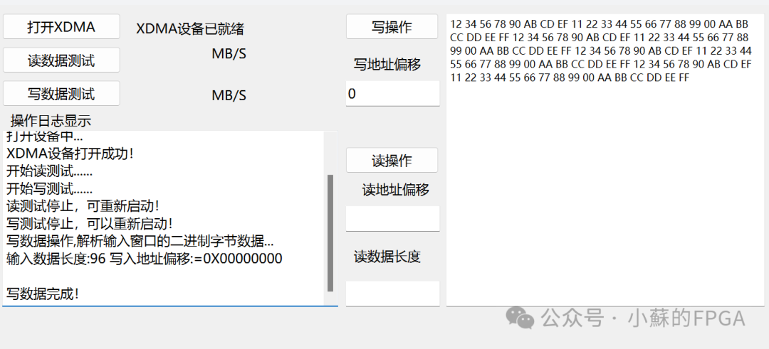
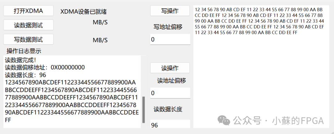
Host write/read data test: The 96 Byte data read/write at the corresponding address is consistent.
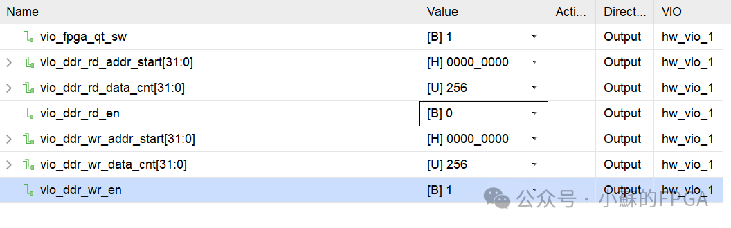
Host write data, FPGA read data test: After the above operations, read the DDR data content through VIO control: The data content is consistent with the 96 Byte data written by the host computer.
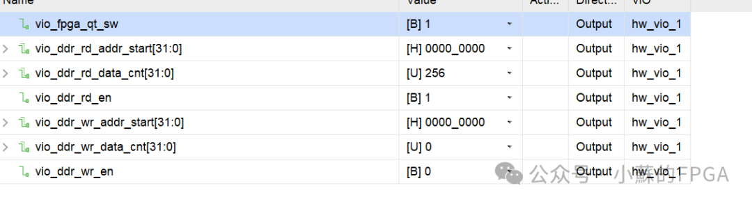
FPGA write DDR and host read test: VIO control writes 256 incrementing 32bit data starting from address 0:
06
—
Extended Applications
Based on the above framework, enabling the XDMA AXI-Lite interface allows interaction with registers or read/write process status through BRAM or GPIO, and applying interrupt functionality can be used in various practical scenarios.
Previous Recommendations:
FPGA Implementation of Aurora Optical Communication Applications
USB 3.0 Implementation Based on FPGA (CYUSB3014)
Ethernet Flow Control Technology Implementation Based on FPGA
Multiphase DDS Waveform Generation Engineering Applications
Broadband Signal Multiphase Filtering and Pulse Compression Processing (FPGA + ADC)
Implementation of AES128 Encryption and Decryption Based on FPGA