A previous article summarized the industrial HART bus, and today we will discuss the RS-485 bus. RS-485 is a widely used communication interface, and this article will cover the key points in detail, with a length of about 5000 words.
The Past and Present
RS-485, what does RS mean? It stands for Recommended Standard, which means a recommended standard. 485 is the standard identification number, and there is no need to delve into why this identification number was set. RS-485 is also known as ANSI/TIA/EIA-485; these prefixes are abbreviations for standard associations, such as EIA, which stands for the Electronics Industries Association. In 1983, the RS-485 communication interface was approved by the Electronics Industries Association as a communication interface standard.Even in today’s booming IoT era, RS-485 still has a large number of applications. Many protocols use RS-485 as the physical layer. What are some commonly used standard protocols that utilize RS-485 as the physical layer? For example:
Industrial HART bus
Modbus protocol
Profibus DP
…….
Electrical Characteristics
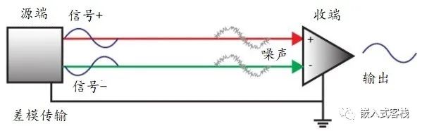
Signal sampling uses differential mode transmission, which contrasts with common mode. Differential mode is also known as differential transmission. So, what does differential mode transmission look like? A picture is worth a thousand words; just look at the two diagrams below:
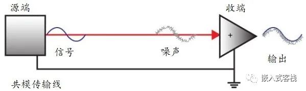
Common Mode Transmission
When using common mode transmission, common mode noise will superimpose on the final output signal, contaminating the original signal.
Differential Mode Transmission
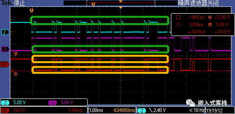
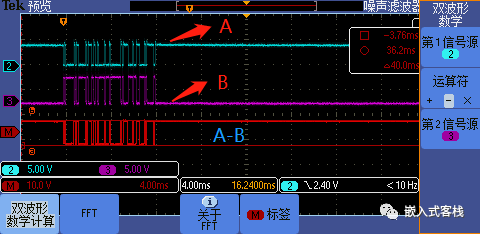
In contrast, when using differential mode transmission, the signals + and – emitted from the source are out of phase. For common mode noise, it exists on both the + and – lines. Ideally, they are equal in amplitude and in phase, and at the receiving end, it acts like a subtractor. The useful signal, being out of phase, is preserved after subtraction, while noise is canceled out. In actual circuits, it will be significantly attenuated.Thus, it is evident that differential mode transmission has advantages over common mode transmission, as it can effectively cancel common mode interference.Differential mode is sometimes referred to as balanced mode, while common mode is also known as unbalanced mode.To illustrate this interference, let’s capture a waveform:At the edges of the A/B signals, the waveforms are slightly distorted, but when you look at A-B (the red line represents the oscilloscope’s MATH subtraction function), the edges become very clean! This example illustrates how differential mode transmission can effectively resist common mode interference.
Electrical Parameters
The electrical parameters of RS-485 are as follows:
Common mode voltage range: -7 to +12V
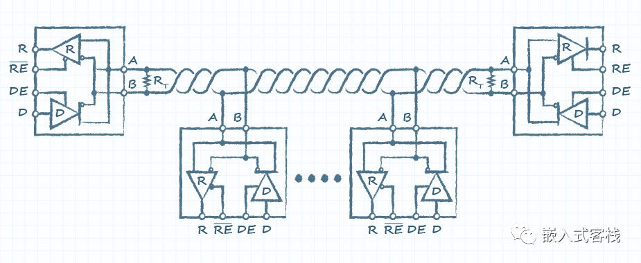
Supports up to 32 multipoint topologies, as shown in the network topology diagram below
When using a 40-foot cable, transmission rates can reach 10Mbps; 1 foot is equivalent to 30.48cm, and Mbps means megabits per second
When using a 4000-foot cable, transmission rates can reach 100kbps
Half-duplex communication
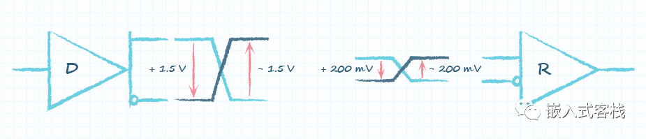
Minimum differential voltage tolerance: 200mV, meaning that if the differential voltage at the receiving end is below 200mV, it cannot correctly identify 0/1. How should this statement be understood?
How should the above diagram be understood? The RS-485 transceiver’s sending circuit must provide at least 1.5V differential voltage output capability. Due to bus line impedance attenuation, 32 receiving circuit input impedances, and the 120Ω terminating resistor, the differential signal’s amplitude will inevitably attenuate. Therefore, at the far end, at least 200mV of differential voltage must be provided to the terminal receiving circuit.
: For the receiving circuit, it judges the difference between the common mode voltage of line A and line B:
If , the receiving circuit R recognizes it as logic 1
If , the receiving circuit R recognizes it as logic 0
In simple terms, if the absolute voltage value of line A is at least 200mV greater than that of line B, it is recognized as logic 1; or if the absolute voltage value of line A is at least 200mV less than that of line B, it is recognized as logic 0
The parameters here should be theoretical values under certain characteristic impedance cables, and adjustments and field testing need to be made during actual engineering use. It is generally advisable not to exceed this theoretical limit.Speaking of electrical characteristics, let’s first take a look at a typical interface circuit:From this interface circuit, there are several key points:
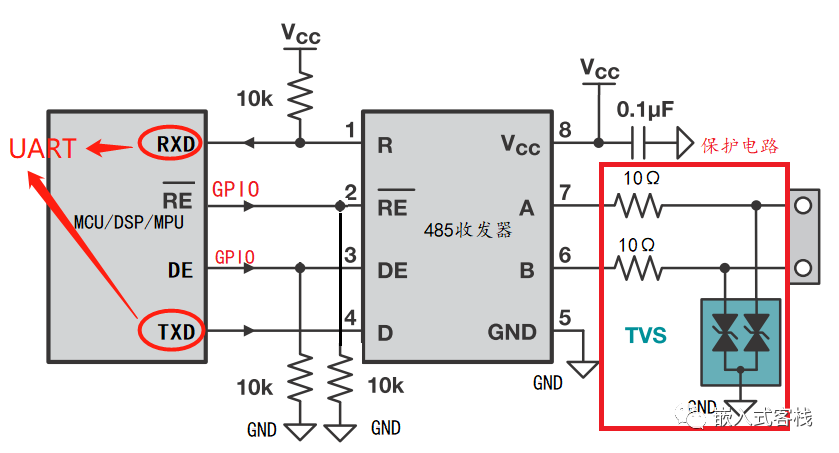
RS-485 communication, from the perspective of the microcontroller/DSP/processor interface, utilizes the UART interface with the RS-485 transceiver interface. Of course, you might ask, can I use FPGA? Certainly, it’s possible to implement a serial transceiver IP module with FPGA. Even if you want to simulate UART with GPIO, it can be done, but it is not very meaningful as it requires CPU resources to implement the low-level BIT transmission.
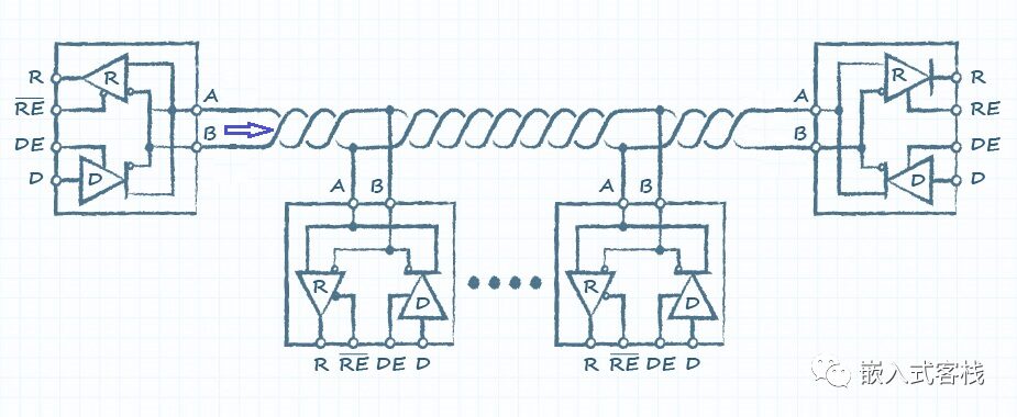
As mentioned before, half-duplex means there is half-duplex and full-duplex. What is half-duplex? First, half-duplex and full-duplex must be defined in a point-to-point context. Here point-to-point means at the same time, where half-duplex means the device can either be in data receiving mode or data transmitting mode, but not both simultaneously.Full-duplex, on the other hand, allows simultaneous transmission and reception. For example, the I2C bus is a half-duplex bus, while the 4-wire SPI is full-duplex, and the 3-wire SPI is also a half-duplex bus; RS-422 or RS-232 are full-duplex interfaces; CAN bus is a half-duplex bus. RS-485 is a type of half-duplex bus:
When the Host sends data, the data travels along the red line through the twisted pair to the Slave’s differential receiving circuit. When the slave responds, the data travels in the blue direction back to the Host’s receiving circuit. However, since the transmission medium is a pair of twisted wires, one side cannot transmit signals while the other is sending data. From the transceiver’s control perspective:A GPIO pin is used to control the transmit/receive enable. A block diagram of the internal principle of the chip makes this easy to understand:
When DIR=0, the receiving circuit is enabled, and the sending circuit is disabled (DE=0), which is equivalent to high impedance on the bus; when DIR=1, the receiving circuit is enabled and the sending circuit is disabled (DE=1), depending on the signal from DI for the A/B signals. Here are two questions:
1. Why does the chip design as opposite effective logic? This is actually convenient for controlling the transmit/receive circuit with a single GPIO.
2. Why not make the transceiver chip’s transmit/receive enable a single pin, for example, just call it DIR? Making it two pins for send/receive can also be controlled separately, such as :
It is even possible to set DE=1 to 0 when DE=1, which could achieve self-looping. This design can also implement self-diagnosis of the transceiver and wiring by comparing received and transmitted messages, thus diagnosing soldering issues, transceiver damage or disconnection, and wiring short circuit faults.However, you might say, this is contradictory! You said earlier that RS-485 cannot transmit and receive simultaneously, but here you say it can. This is not contradictory; the earlier statement about not being able to transmit and receive simultaneously refers to not being able to receive messages from other devices while transmitting.
Therefore, the essence of half-duplex communication is that the communication medium does not have a bidirectional channel. When sending data to the bus, the medium is occupied, and even if you want to send, you cannot correctly transmit the signal onto the medium. If you force transmission, the data will become disordered, and the transceiver chip may even be damaged.
: Receiver Output Enable, enabling the receiver,
DE: Driver Output Enable, enabling the driver output
The DIR pin in the diagram controls whether the current RS-485 is in “receive” or “transmit” mode.
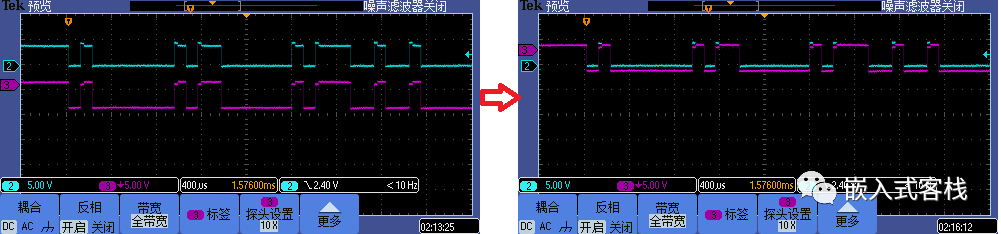
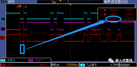
Earlier, we discussed common mode voltage specifications and differential mode transmission. Now, let’s capture the waveform:The oscilloscope’s CH2 connects to the 485 output A terminal, and CH3 connects to the 485 output A terminal. The red line is the oscilloscope’s MATH function: CH2-CH3. Most oscilloscopes have mathematical operation capabilities.If you want to view the differential signal, you can use a dual-channel oscilloscope with the MATH subtraction function. If some oscilloscopes lack the MATH function, you can use a trick:Invert the negative terminal of channel B, or the differential signal, and then align it with the idle level; this makes it easier to observe A-B, right?From this diagram, what valuable signal characteristics can we discover?
Signal A is high when idle; signal B is low when idle. Therefore, you will see devices labeled 485_A+ and 485_B-.
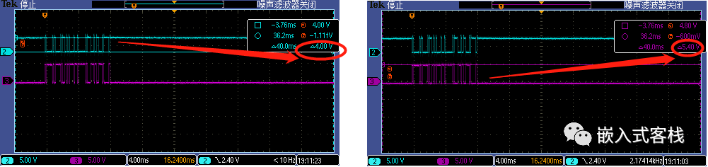
The common mode voltage values of each channel are within the standard requirements of -7 to 12V, with signal A at 4V and signal B at 5V:
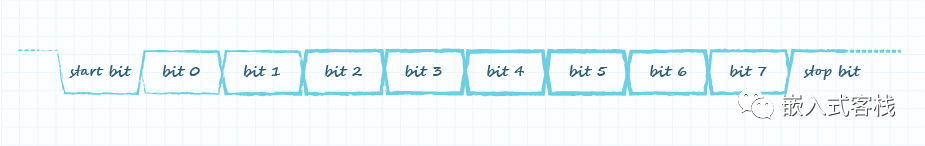
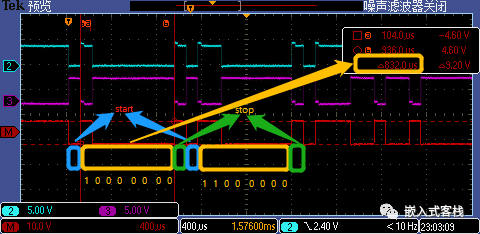
So how should the data be interpreted?The captured data is a MODBUS-RTU master sending to a slave device, with the first two bytes being 0x01 0x03. The UART mode has 1 start bit, 8 data bits, 1 stop bit, no parity, and low byte first. In this case, the UART communication format is:First, based on the UART communication mode, let’s calculate several parameters: the time occupied by each bit and the time occupied by each byte:This diagram shows that the width of the start bit is exactly 104us.For parsing asynchronous serial timing waveforms, the most important thing is to calculate bit time and byte time based on the communication format, which allows direct waveform data parsing. From this perspective, if you want to use FPGA to implement a UART protocol logic analyzer, this is the core indicator. By detecting the start bit edge, you can parse the data along the time axis. Here, I’ll act as a visual UART logic analyzer:The time width of the 8-bit data is exactly 832us. Since the format is low byte first, we need to look at it in reverse; it matches the actual sent data 0x01 0x03.This method can be used to check if the software correctly drives the hardware when debugging the low-level system. For instance, when debugging I2C/SPI and other low-level interfaces, similar methods can be used to check hardware waveforms. The only difference is that I2C/SPI belong to synchronous communication, which means their communication layer has a synchronous clock signal; SCL for I2C and SCK for SPI are synchronous clocks.
Driving Capability
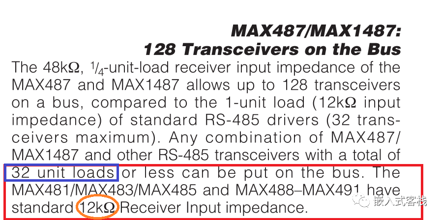
The electrical parameters summarize that the maximum electrical driving capability of RS-485, under a multipoint network topology structure, can drive up to 32 stations. How should this specification be interpreted?First, let’s examine the characteristics of a station’s transceiver circuit; the standard equivalent input impedance of the receiver circuit is 12kΩ, for example, based on the MAX 485 data sheet:Why is it 32? It is mainly due to the earlier specification of the minimum driving capability of 200mV.This can also be understood as follows: each receiving circuit input impedance is not ideally high, but 12kΩ. So if one of the stations sends, it is equivalent to having 32 stations’ input impedances in parallel. Why 32? Don’t forget that the sending station itself also has a receiving circuit. Therefore, neglecting the terminating resistor and line impedance, the sending circuit is connected to an equivalent load, and the driving capability of the sending circuit is limited, which makes it easier to understand.The following diagram illustrates the so-called multipoint network topology, where all stations are connected along the twisted pair.Therefore, you may see terms like “one unit RS-485 load” in some places. This so-called unit load refers to the 12kΩ standard input impedance, which is defined by the EIA-485 standard. Thus, when you see terms like unit load, it originates from this concept.
Data Monitoring
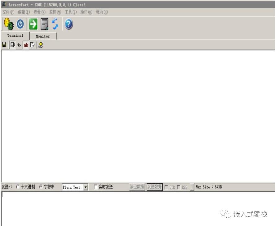
For example, in a Modbus-RTU multipoint network based on RS-485, when programming protocols or debugging actual multi-station buses, it may be necessary to monitor all messages on the bus. It is also possible to implement a bus message recorder to log all messages on the bus. How can this be achieved?Purchase a USB to RS-485 converter or make one yourself. Connect the A/B lines to the bus and plug the USB into the computer. Use a serial monitoring terminal or write a small serial receiving software to monitor all messages on the bus.For instance, this AccessPort serial tool is quite useful:
Application Design
In application design, these dimensions need to be considered:
Termination design
Interface chip
Isolation design
Termination Design
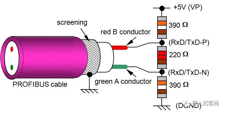
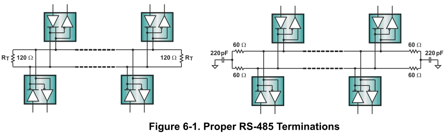
First, why is termination necessary? This is because RS-485 uses twisted pair transmission, and the standard specifies that the differential characteristic impedance of twisted pairs is between 100Ω and 150Ω. The RS-485 standard designers chose 120Ω as the nominal characteristic impedance.Assuming the signal is sent from the left station, if there is no termination, the signal’s impedance is continuous while traveling through the line, but when it reaches the right side, the equivalent impedance becomes the input impedance of the receiving circuit, which may be 12kΩ. The impedance becomes discontinuous, leading to an impedance mismatch! A portion of the signal energy will reflect back along the original path, and due to capacitance and inductance, a phase difference will occur. The reflected signal will superimpose with the original signal, causing communication errors; in severe cases, communication may fail entirely.To gain a deeper understanding of the underlying principles, one can study transmission line theory.Some friends who have worked with Profibus DP (which also uses RS-485 as the physical layer) may wonder why the recommended termination circuit for Profibus DP looks like this:This is because the communication medium used in Profibus DP has a different nominal characteristic impedance. Therefore, there may be slight differences in practical engineering applications.In TI’s documentation, I found this termination method:In environments with significant noise, it is recommended to use the termination scheme on the right, which utilizes two 60Ω resistors and a 220pF capacitor to form a low-pass filter, increasing the line’s noise immunity.When wiring in actual engineering, if you encounter significant noise, you can use an oscilloscope to check the bus signal quality and make minor adjustments to the termination method.
Interface Design
Many chip manufacturers, such as TI and Microchip, provide RS-485 transceiver chips. When selecting an interface chip, consider whether the chip’s supply voltage input logic is compatible with the levels of the microcontroller/DSP being used. Additionally, consider whether the input impedance of the receiving circuit meets the RS-485 standard input impedance. If not, the number of loads that can be supported during network deployment may need adjustment. Also, note that some new designs of RS-485 transceivers feature fail-safe functionality.Moreover, as mentioned earlier, standard transceivers can drive up to 32 standard transceiver load devices, which means (12kΩ) standard unit input impedance.When designing specific interface circuits, EMC requirements should also be considered. In some device settings, there can be strong interference, such as large inductive devices running on the power grid; this can sometimes interfere with the equipment. Additionally, there may be spatial radiation interference. In such cases, consider using shielded twisted pairs, with the shielding connected to ground. My knowledge of interference resistance is not very deep, but I’ve organized some points. Here’s a lightning protection interface circuit design solution for reference:https://www.programmersought.com/article/95833359295/Earlier, it was mentioned that standard RS-485 can accommodate 32 standard receiving impedance transceiver devices. What to do if you want to connect more than 32 station devices in the actual system? You can design a relay device. This is like connecting two network segments using a relay to solve the driving capability issue. Of course, there are ready-made products available for this.
Isolation Design
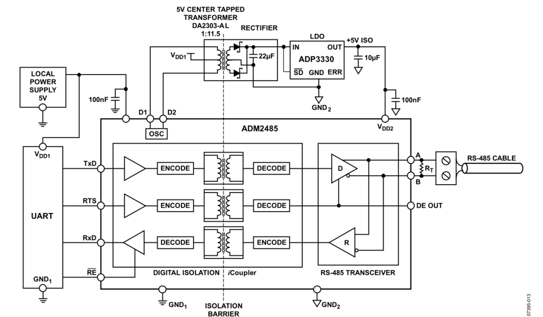
Why is isolation necessary? It is to reduce ground noise. In many settings, there may be large current switching devices, inductive devices like motors, etc., and noise can easily couple into the device through the communication ground. Especially in industrial equipment, interfaces are usually designed to be isolated. When designing isolated interfaces, consider choosing chips with isolation functionality, such as ADI’s iCoupler technology products like ADM2481 and ADM2485. Alternatively, you can use optocouplers with standard RS-485 transceivers. The only thing to note is that you need to design an isolated power supply to power the circuits on both sides of the isolation.The above diagram is from TI’s “The RS-485 Design Guide,” which is quite good. Many parts of this article were also organized based on this documentation. If you are interested in this material, you can reply with 485 to receive it automatically.
In Summary
RS-485 may seem simple, but there are many aspects to understand and pay attention to in actual application design. Creating a robust product often hinges not on the overall direction but on small details that can easily lead to product instability.
Recommended to follow 👇 the public account below to learn more about electronic technology knowledge!
Bluetooth: Why is it called “Bluetooth” and not “White Tooth”?
Hard-earned C language notes, glad I didn’t give up
Do you call this junk a CPU?
Multimeter burned out, disassembled, and miraculously repaired it!
Popular Science | Understand in 30 seconds, the world’s most powerful chip companies!
Hardware reliability and improvement
SVPWM algorithm principles and detailed explanation