This article is a guide.
1. Application Issues
When communication errors or failures occur, first check if the application meets the conditions listed in Table 1.
Table 1 RS-485 Bus Application Conditions
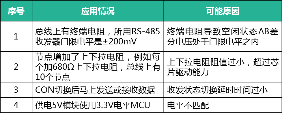
The three application conditions in Table 1 relate to terminal resistors, pull-up/pull-down resistors, control pins, and logic input side levels. Below is a detailed analysis.
1. Terminal Resistor Issues
If terminal resistors are connected on the RS-485 bus, and the threshold level of the RS-485 transceiver is ±200mV, the abnormal phenomena described in Table 2 may occur.
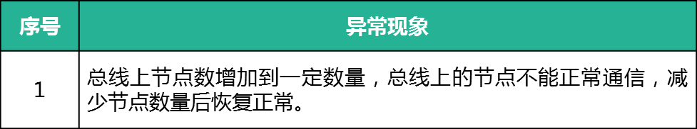
Table 2 Abnormal Phenomena Caused by Terminal Resistors
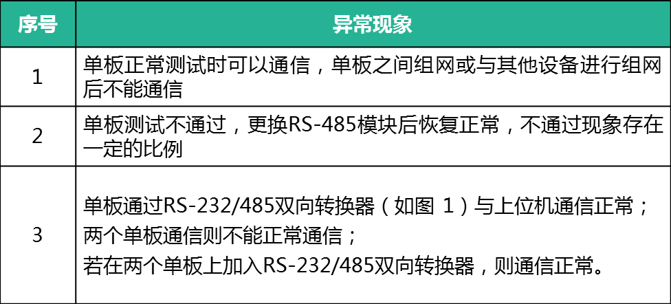
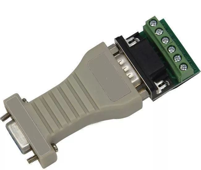
Figure 1 RS232/485 Bi-directional Converter
Reasons for Abnormalities Caused by Terminal Resistors: The receiving threshold level of the RS-485 transceiver is ±200mV, meaning that if the differential voltage between A and B exceeds +200mV, a high level is output; if it is below -200mV, a low level is output. When the voltage between A and B is within ±200mV, the output state is uncertain, which can result in either a high or low output level. Thus, if the differential voltage between A and B is within the threshold level during idle state, abnormal issues may occur with a certain probability.
Analysis of Phenomenon 1 in Table 2: The single board can communicate normally, but after networking, the presence of terminal resistors on the RS-485 bus causes the differential voltage during idle state to be within the threshold level, leading to communication issues. When this situation arises, first confirm whether there are terminal resistors on the bus.
Analysis of Phenomenon 2 in Table 2: During the single board test, if the board or the communicating device has terminal resistors connected, the differential voltage between A and B may be within the threshold level, leading to communication errors.
Analysis of Phenomenon 3 in Table 2: This phenomenon is also caused by terminal resistors. The RS-232/485 bi-directional converter (as shown in Figure 1) typically has small-value pull-up and pull-down resistors (e.g., 560Ω) internally. When communicating using the RS-232/485 bi-directional converter, the voltage during idle state is determined by the voltage divider formed by the pull-up/pull-down resistors and terminal resistors. In this case, the differential voltage during idle state will be greater than 200mV, ensuring that the RS-485 transceiver outputs a definite high level, thus avoiding communication errors. For example, in Figure 3, two RSM485PCHT modules communicate with a 60Ω resistor added between A and B, and the test waveform shows that the idle state voltage is 520mV, which will not cause errors. In Figure 2, two RSM485PCHT modules communicate with a 60Ω resistor added, and the waveform shows that the idle state differential voltage between A and B is 40mV, which is within the threshold level range, leading to potential communication errors.
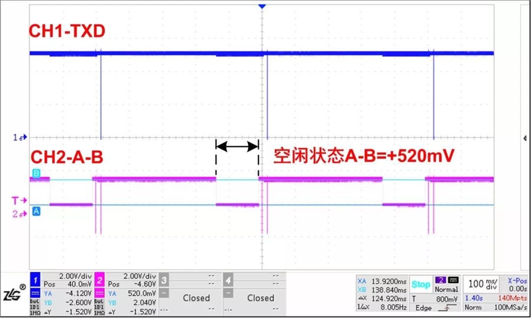
Figure 2 Adding two 120Ω resistors between A and B, along with RS-232/485 bi-directional converter
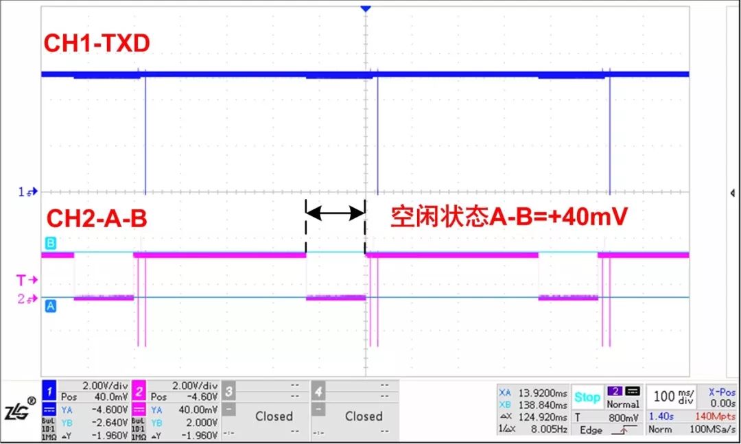
Figure 3 Only adding two 120Ω resistors between A and B
The solutions mainly include three methods, as detailed in Table 3:
Table 3 Solutions for Terminal Resistor Issues

2. Pull-up/Pull-down Resistor Issues
Small parallel values of pull-up and pull-down resistors may cause phenomena as shown in Table 4.
Table 4 Abnormal Phenomena Caused by Pull-up/Pull-down Resistors
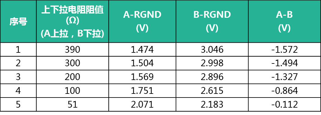
The above issues are caused by the small values of the added pull-up and pull-down resistors, which exceed the load capacity that the chip can drive. After adding two 120Ω resistors between A and B in the RSM485PCHT, the relationship between the added pull-up/pull-down resistor values and the output differential voltage low level is shown in Table 5. When the parallel value of the pull-up/pull-down resistors is less than 51Ω, although the chip can output normally, the output signal may exceed -200mV, leading to possible communication errors or complete communication failure. Small pull-up/pull-down resistor values can cause the RS-485 transceiver to draw excessive power, leading to severe heating, potentially triggering overheat protection or damage. Therefore, to ensure reliable communication, the values of pull-up and pull-down resistors should not be too small; typically, the parallel value should be greater than 375Ω.
Table 5 Driving Voltage with Different Pull-up/Pull-down Resistor Values
3. Control Pin and Logic Input Side Issues
Due to the need for a certain delay in transceiver switching, a delay (e.g., at least 25μs for RSM485PCHT) should be added before sending or receiving data to ensure that the RS-485 transceiver is in the sending or receiving state.
The MCU level should match the RS-485 transceiver’s input logic level. For example, if the MCU operates at 5V logic level, a 5V powered RSM series isolation module should be used.
2. Waveform Testing Methods
As the RS-485 bus is widely used, application issues are not limited to the above cases. After excluding the aforementioned problems, testing the bus waveform can help locate communication anomalies and determine the cause.
1. Check the Sending Function of the RS-485 Transceiver
During communication anomalies, measuring the corresponding relationship between the RS-485 bus AB differential voltage and the module TXD, RXD pin waveforms can help identify the anomaly location. Using the testing method shown in Figure 4 yields the waveform shown in Figure 5. When TXD is high, A-B is high; when TXD is low, A-B is low, and if the module output level is normal, it can be determined that the module sending function is normal.
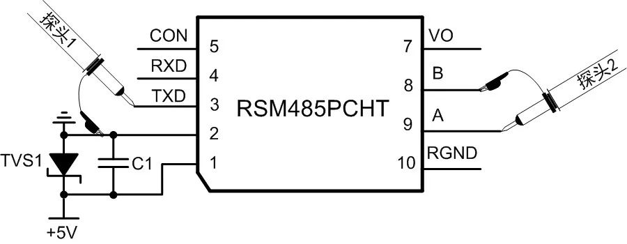
Figure 4 Testing if the Sending Function is Normal
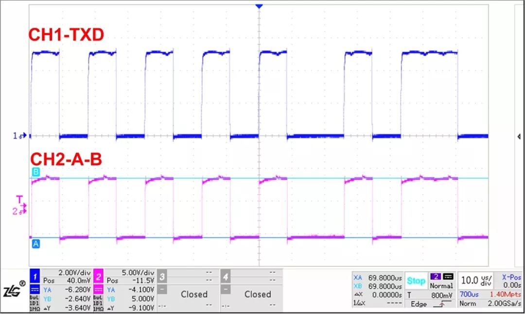
Figure 5 Normal Waveform for Sending Function Test
2. Check the Receiving Function of the RS-485 Transceiver
Using the testing method shown in Figure 6 yields the waveform shown in Figure 7. When A-B is high, RXD is high; when A-B is low, RXD is low, and if the module RXD output level is normal, it can be determined that the module receiving function is normal.
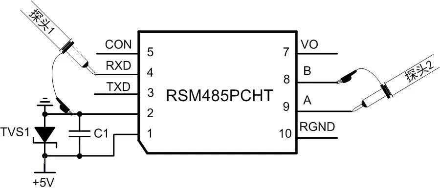
Figure 6 Testing if the Receiving Function is Normal
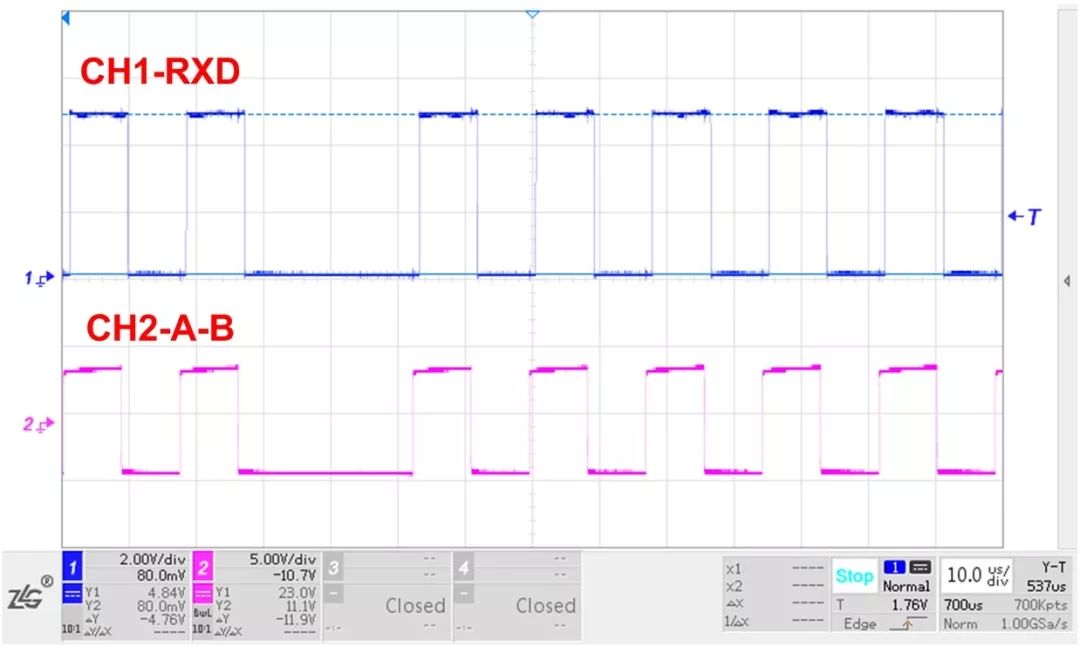
Figure 7 Normal Waveform for Receiving Function Test
3. Check the Control Pin and TXD, RXD Logic Relationship of the RS-485 Transceiver
Using the method shown in Figure 8, test the logic relationship between TXD, RXD, and CON to obtain the waveforms shown in Figures 9 and 10. For the RSM485PCHT, the CON pin should be set low or high at least 25μs before sending or receiving signals, and the transceiver state should only be switched after data transmission or reception is completed.
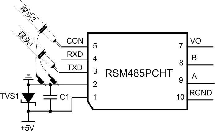
Figure 8 Testing TXD and CON
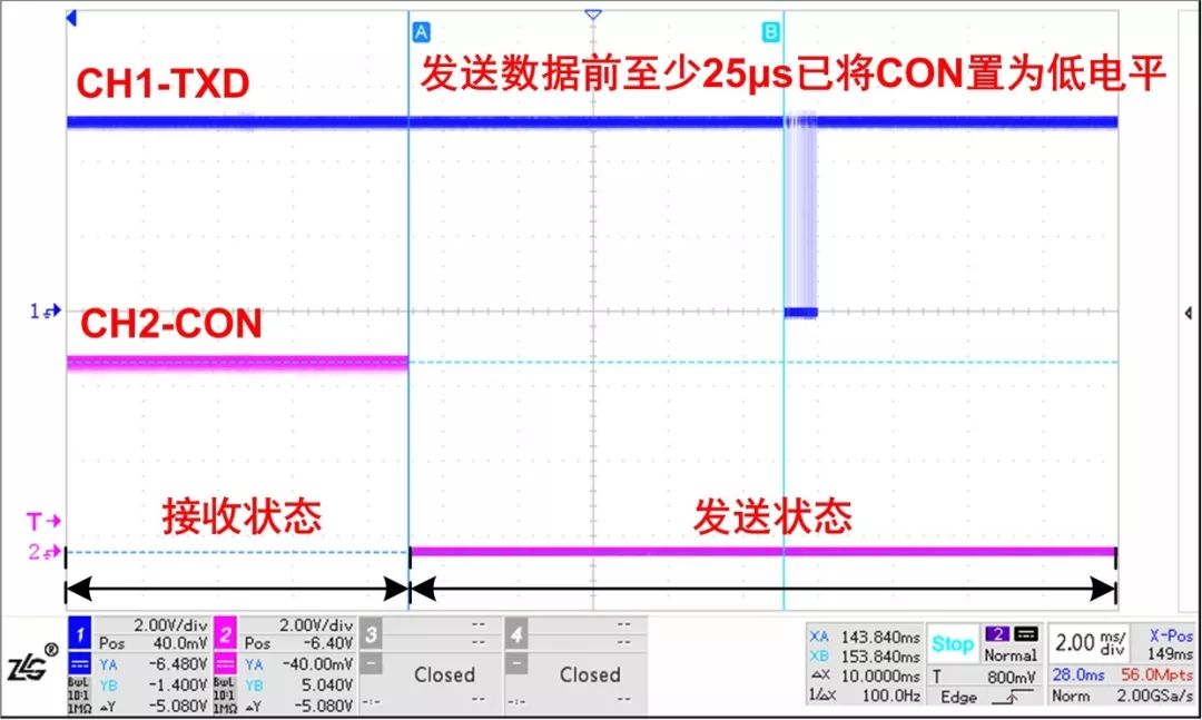
Figure 9 Data Sending CON Waveform
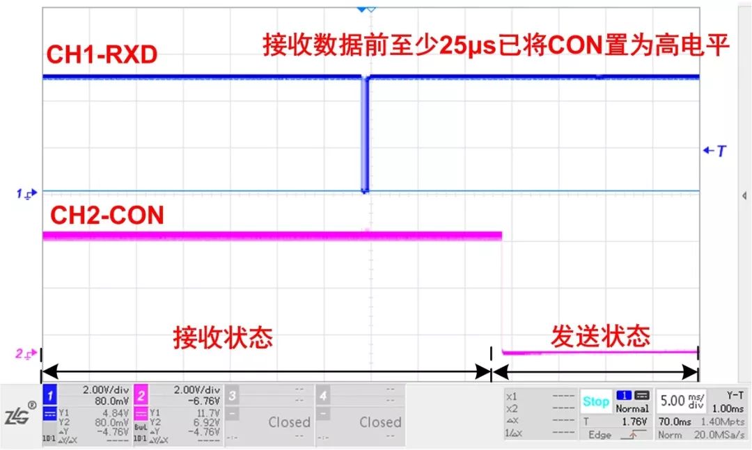
Figure 10 Data Receiving CON Waveform
3. Transceiver Damage
1. Damage Caused by AB Pins Exceeding Common-mode Voltage Range
The common-mode voltage range for the AB pins of the RS-485 transceiver is generally required to be within -7V to +12V. Exceeding this range can cause chip damage. In industrial environments, large instantaneous currents often flow through the ground, and if the transceiver RGND pin is improperly connected, the common-mode voltage at the AB pins can exceed the permissible range, leading to module damage. Below is an analysis using the RSM485PCHT as an example.
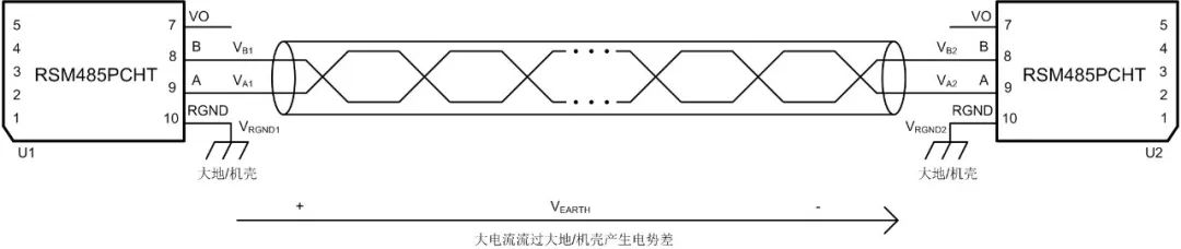
Figure 11 Incorrect Connection of RGND to Ground
When U1 sends a high level, taking RSM485PCHT as an example:
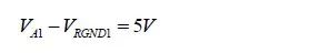
Since both modules are directly connected to the chassis or ground, when a large current flows through the chassis or ground, a voltage difference VEARTH is generated between the RGND pins of U1 and U2. When U1 sends data to U2, the voltage at U2’s A pin is:
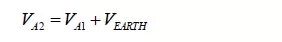
When VA1 is 5V during transmission, if VEARTH exceeds 7V, it may cause damage. Therefore, in practical applications, the RGND between nodes can be connected through the shielding layer of the twisted pair cable, with the shielding layer connected to the ground through a resistor-capacitor single-point connection, as shown in Figure 12.
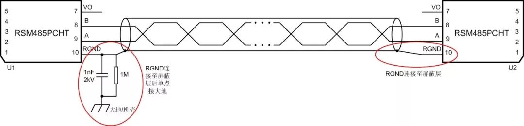
Figure 12 Recommended Connection of RGND
2. Damage Caused by High Levels of Electrostatic Discharge and Surge
In environments with high levels of electrostatic discharge and surge, simply using RS-485 transceiver chips or modules may lead to module damage. In such cases, additional protective circuits are needed to safeguard the transceiver. However, the protective circuit must be reliably grounded to dissipate the energy from electrostatic discharge and surge. Below is an example of common-mode surge testing, as shown in Figure 13. If the protective circuit is not connected to ground, the surge energy (red section) is released through the isolation module, and high surge levels may easily damage the module. When the protective circuit is grounded, as shown in Figure 14, the surge energy first dissipates to ground through the GDT, then through the TVS and capacitor, leaving very little energy to be released through the module, thus providing protection.
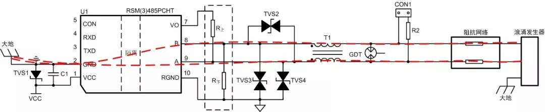
Figure 13 Protective Circuit Not Grounded
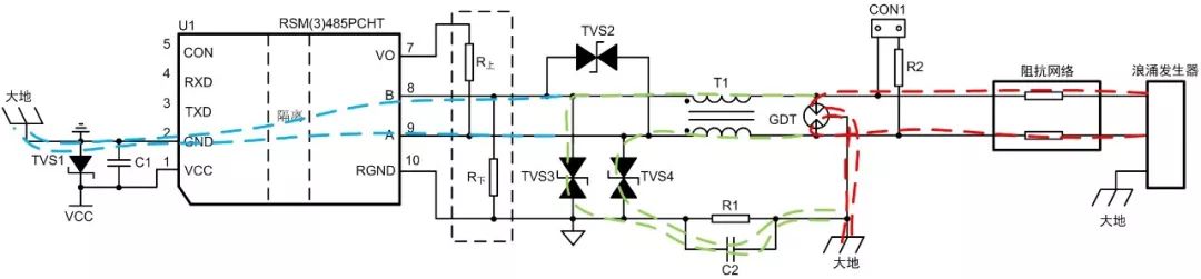
Figure 14 Protective Circuit Grounded
For more technical topics, reply with the keyword 【power supply】.
Official WeChat Account Introduction
The official WeChat account of Zhiyuan Electronics, a research and development sharing platform with 500 engineers, providing you with leading products and solutions in the electronics industry..