Let’s learn about the composition, design, process, workflow, and principles of component placement and routing for PCB circuit boards, along with some considerations for the later stages!
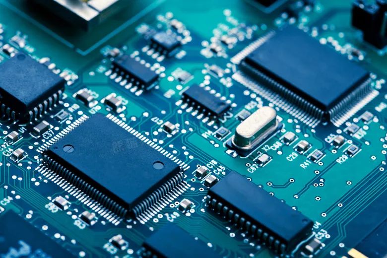
Composition of PCB Circuit Boards
1. Lines and Planes: The lines serve as the conductive paths between components, and a large copper area is designed separately for grounding and power layers. The lines and planes are created simultaneously.
2. Dielectric Layer: This layer maintains insulation between the lines and various layers, commonly referred to as the substrate.
3. Holes: Through-holes allow connections between two or more layers, while larger through-holes are used for component insertion. Non-conductive holes are typically used for surface mount positioning and securing screws during assembly.
4. Solder Mask Ink: Not all copper surfaces require soldering components; thus, a layer of material (usually epoxy resin) is printed over non-solder areas to prevent short circuits between non-soldered lines. Depending on the process, it can be categorized as green ink, red ink, or blue ink.
5. Silkscreen: This is not a necessary component but serves the primary function of labeling the names and positions of components on the circuit board for easier maintenance and identification after assembly.
6. Surface Treatment: Copper surfaces are prone to oxidation in normal environments, leading to poor solderability. Therefore, protective measures are taken on the copper surfaces that will be soldered. Protection methods include tin spraying, gold plating, silver plating, tin plating, and organic solderability preservatives, each with its advantages and disadvantages, collectively referred to as surface treatment.
Design Steps for PCB Circuit Boards
1. Design of the Circuit Schematic: The circuit schematic is primarily drawn using the schematic editor in Protel DXP.
2. Generate Netlist: The netlist displays the connection relationships between the components in the circuit schematic, serving as a bridge between the schematic design and the PCB design. It allows for quick identification of relationships between components, facilitating subsequent PCB design.
3. PCB Circuit Board Design: PCB design is based on the circuit schematic to achieve the required functionality. Designing the PCB layout involves considering many factors, including mechanical structure, external connection layout, component placement, wiring, heat dissipation, and electromagnetic compatibility. Completing this step often requires numerous modifications to the circuit schematic.
4. PCBA Control Board Production: After purchasing components and receiving the PCB, the various components are soldered onto the board according to the schematic through SMT assembly and DIP insertion processes, completing the control board.
Principles of Component Placement
First, place components that closely fit the structure, such as power sockets, indicator lights, switches, connectors, and interfaces; next, place special components like large, heavy, or heat-generating components, and finally, place smaller components. When laying out components, consider routing to choose layouts that facilitate wiring.
1. Crystal oscillators should be placed close to the IC;
2. The layout of decoupling capacitors should be as close as possible to the power pins of the IC, minimizing the loop formed with power and ground;
3. Heat-generating components should be evenly distributed to facilitate heat dissipation for both the single board and the entire device, and temperature-sensitive components should be kept away from high-heat components;
Routing Principles
1. High-speed signal traces should be kept as short as possible, and critical signal traces should also be kept short;
2. A single trace should not have too many vias, ideally no more than two vias;
3. Trace corners should be greater than 90 degrees whenever possible, avoiding corners below 90 degrees and minimizing the use of 90-degree corners;
4. When routing double-sided boards, traces on both sides should be perpendicular, diagonal, or curved to avoid parallel routing, which reduces parasitic coupling;
5. Audio input lines should be of equal length, placed close together, with audio lines shielded by ground lines;
6. No traces should run under power amplifier ICs, and multiple vias should connect to GND beneath the power amplifier IC;
7. In double-sided boards without a ground layer, the ground line for the crystal oscillator capacitor should use the shortest possible trace to connect to the nearest GND pin of the device, minimizing vias;
8. Power lines and USB charging inputs should use thick traces (>=1mm), with copper poured at via locations and multiple vias at the copper pour;
In general, power and ground lines should be routed first to ensure the electrical performance of the circuit board. Where conditions permit, the width of power and ground lines should be increased, ideally with ground lines wider than power lines. Their relationship is: ground line > power line > signal line, with typical signal line widths of 0.2-0.3mm, and the minimum width can reach 0.05-0.07mm, while power lines generally range from 1.2-2.5mm.
Complete Manufacturing Process for Multilayer PCB Circuit Boards
1. Inner Layer: This is primarily for creating the inner layer circuits of the PCB circuit board;
Manufacturing process: (1) Cutting the board: Cut the PCB substrate to the production size; (2) Pre-treatment: Clean the surface of the PCB substrate to remove surface contaminants; (3) Lamination: Apply dry film to the surface of the PCB substrate in preparation for image transfer; (4) Exposure: Use exposure equipment to expose the coated substrate with UV light, transferring the image to the dry film; (5) Development: The exposed substrate undergoes development, etching, and film removal to complete the inner layer board production.
2. Internal Inspection: This is primarily for inspecting and repairing the board’s circuits; AOI: AOI optical scanning can compare the PCB board’s image with the data of a known good board to identify defects such as gaps and dents; VRS: The defective image data detected by AOI is sent to VRS for repair by relevant personnel; repair: Gold wire is soldered onto gaps or dents to prevent electrical issues;
3. Lamination: This involves laminating multiple inner layers into a single board; Browning: Browning increases the adhesion between the board and resin, as well as the wettability of the copper surface; riveting: Cut the PP into small and standard sizes to match the inner layers; stacking, pressing, drilling, and edge milling;
4. Drilling: Drill holes of varying diameters as required by the customer using a drilling machine, allowing for through-holes between boards for subsequent processing and component insertion, which also aids in heat dissipation;
5. First Copper: Copper plating is applied to the drilled holes in the outer layer board to ensure connectivity between the layers; burr removal: Remove burrs from the edges of the holes to prevent poor copper plating; glue removal: Remove glue residue from inside the holes to enhance adhesion during micro-etching;
6. Outer Layer: The outer layer process is similar to the first step of the inner layer process, aimed at facilitating subsequent processes for creating circuits;
7. Second Copper and Etching: Second copper plating and etching are performed;
8. Solder Mask: This protects the board from oxidation and other issues;
9. Text: Printing text; acid washing: Clean the surface of the board to remove oxidation and enhance the adhesion of the printed ink;
10. Surface Treatment OSP: The side of the bare copper board that will be soldered is treated with a coating to form an organic film, preventing rust and oxidation;
11. Shaping: Shape the board to the required specifications for SMT placement and assembly;
12. Flying Probe Testing: Test the board’s circuits to avoid short circuits before release;
13. FQC: Final inspection, conducting a full check after completing all processes;
14. Packaging and Shipping, completing delivery.
Considerations for PCB Circuit Board Manufacturing Process
1. The outline of the circuit board should be drawn using the keep-out layer;
2. The spacing between lines, between lines and vias, and the spacing of copper pours must meet the requirements of the fabrication plant, generally 10 mils;
3. Conduct a rule check before submitting the board, focusing on detecting shorts and opens;
4. Components should be placed at least 2mm away from the board edge.


Screenshots of Some E-books from the 300G Collection