Abstract: This design guide discusses several important aspects of the RS-485 standard, aimed at helping engineers design data transmission circuits correctly.
In 1983, the Electronic Industries Association (EIA) approved a new balanced transmission standard known as RS-485. It has been widely praised and applied in industrial, medical, and consumer products, making RS-485 a mainstay in industrial interfaces.
This design guide is intended for engineers who are unfamiliar with the RS-485 standard, providing guidelines for designing RS-485 circuits to help them achieve robust and reliable data transmission designs in the shortest time possible.
Overall, this document discusses the RS-485 standard around the following topics: bus topology, signal levels, cable type, bus termination, failsafe, bus loading, data rate versus bus length, minimum node spacing, grounding and isolation.
RS-485 is merely an electrical standard. Unlike complete interface standards that define functionality, mechanical structure, and electrical specifications, RS-485 only defines the electrical characteristics of drivers and receivers using balanced multipoint transmission lines.
Many higher-level standards reference RS-485 as the standard. For example, China’s multifunctional electric meter communication protocol standard DL/T645 explicitly specifies RS-485 as the physical layer standard.
Key features of RS-485 include:
-
Balanced interface
-
Multi-node sharing a single 5V power supply
-
Bus common-mode voltage range: -7V to +12V
-
Can connect up to 32 loads
-
Maximum 10Mbps (within 40 inches, about 12.2 meters)
-
Longest communication distance of 4000 feet (approximately 1219 meters) at 100Kbps
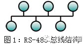
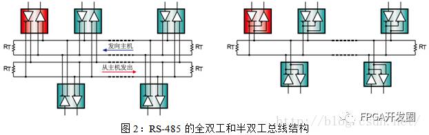
The RS-485 standard recommends a serial networking method for nodes, known as daisy-chain, also referred to as party line or bus topology, as shown in Figure 1. In this topology, drivers, receivers, and transceivers connect to the backbone via short network cables in subnet (or branch) form. The bus interface can be designed as full-duplex or half-duplex, as shown in Figure 2.
Implementing full-duplex requires 2 pairs of signal lines (4 wires), with full-duplex transceivers having separate sending and receiving bus cables. In full-duplex mode, a node can send data while receiving data simultaneously.
In half-duplex mode, only one pair of signal lines is used. Sending and receiving data cannot occur simultaneously. All nodes must be controlled via a direction control signal, such as the driver/receiver enable signal. This ensures that only one driver is active on the bus at any time. If more than one driver accesses the bus simultaneously, it can cause bus contention, leading to data corruption on the bus, thus software control must be implemented throughout the operation to avoid multiple drivers sending data to the bus at the same time.
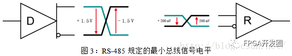
Drivers compliant with the RS-485 standard can provide a differential output of no less than 1.5V (under a 54Ω load), and receivers compliant with the RS-485 standard can detect differential signal inputs as low as 200mV. Even under severely degraded cables and connectors, these values still provide ample margin for high-reliability data transmission. This robustness of RS-485 is why it excels in long-distance networking even in electromagnetic interference environments.
Transmitting differential signals over twisted pairs is advantageous for RS-485 applications, as external interference sources couple equally to both signal lines in a common-mode manner, and this noise is filtered out by differential receivers.
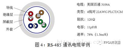
Industrial RS-485 cables are categorized into shielded, unshielded, twisted pair, and unshielded twisted pair, with cables conforming to the American 22-24 AWG wire gauge having a characteristic impedance of 120Ω. Figure 4 shows a cross-section of a 4-wire pair cable, which is typically used for 2 full-duplex networks. Cables containing 2 or 1 pair of signal lines can be used for low-cost half-duplex system designs.
In addition to network wiring, the RS-485 standard mandates that the printed circuit board layout and connectors of devices must be consistent with the electrical characteristics of the network, which can be achieved by keeping the two signal lines on the printed circuit board as close together and of equal length as possible.
To avoid signal reflections, the data transmission line must have endpoints, and the branch length should be kept as short as possible. Proper termination requires termination resistors RT to match the characteristic impedance Z0 of the transmission line. The RS-485 standard recommends a cable Z0 of 120Ω. The cable trunk typically terminates with 120Ω resistors, one at each end. See the left half of Figure 5.
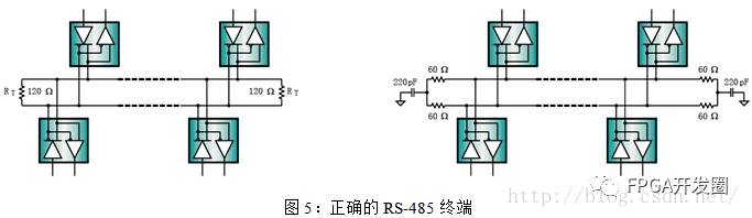
In applications within interference environments, two 60Ω resistors are often used instead of 120Ω resistors to form a low-pass filter, providing additional common-mode interference filtering capability, as shown in the right side of Figure 5. In this case, the pairing of resistor values becomes important (precision resistors of 1% are preferred). Matching resistor values ensure that both filters have the same frequency attenuation; if the resistor precision is low (e.g., 20%), it can cause a difference in the corner frequency of the filters, turning common-mode interference into differential-mode interference, thereby reducing the receiver’s interference tolerance.
The electrical length of the branch (the distance from the transceiver to the cable trunk) should be less than one-tenth of the driver rise time:

Where: LStub = maximum branch length (in feet) tr = driver (10/90) rise time (in ns) v = rate at which the signal travels in the cable relative to the speed of light c = speed of light (9.8*10^8 ft/s)
Table 1 lists the maximum branch lengths when using the cable shown in Figure 4 (v=78%).

Note: Drivers with slow rise times are suitable for applications requiring long branches, and slow rise times can reduce EMI from the devices.
Failsafe ensures that receivers can output a defined state when there is a loss of signal.
Three conditions may lead to loss of signal (LOS): 1. Open circuit: the cable is interrupted or the transceiver is disconnected from the bus 2. Short circuit: the differential signal line cores contact each other due to the failure of the external insulation layer 3. Bus idle: no drivers on the bus are sending signals
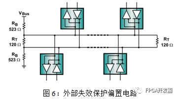
Under the above conditions, when the input signal is zero, traditional receivers would output a random state. However, modern transceivers include a bias circuit that can protect against open circuits, short circuits, and idle buses, allowing the receiver to force a defined state even in case of signal loss.
This failsafe circuit has a drawback: the worst-case noise margin is only 10mV, so in interference environments, external failsafe circuits should be added to increase the noise margin.
The external failsafe circuit consists of a resistor voltage divider that can produce sufficient bus differential voltage to drive the receiver to produce a defined output state. To ensure there is enough noise margin, VAB should include the maximum measured noise: VAB = 200mV + VNoise
The calculation of the failsafe bias resistor value should be based on the worst conditions, namely the maximum noise and minimum supply voltage:

If the minimum bus voltage is 4.75V (5V-5%), VAB=0.25, Z0=120Ω, then RB is 528Ω. The failsafe protection circuit composed of two 523Ω resistors in series with the termination matching resistor RT is shown in Figure 6.
The current output of the driver depends on the load, the transceiver, and the current required by the failsafe circuit. To estimate the maximum number of loads on the bus, RS-485 defines a term: unit load (UL), which represents an impedance of approximately 12KΩ. Standard-compliant drivers must be capable of driving up to 32 such unit loads. Modern transmitters often reduce the unit load, such as only 1/8 UL, allowing up to 256 such transceivers to be connected on the bus.
Since the failsafe circuit can account for a maximum of 20 unit loads, the maximum number of transceivers N is reduced to:

Thus, when using 1/8 UL transceivers, a maximum of 96 such drivers can be connected on the bus.
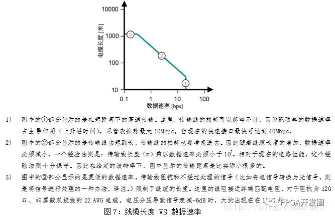
For a given data rate, the maximum bus length is affected by transmission line losses and signal jitter. When the baud period jitter is 10% or more, the reliability of the data drops sharply. Figure 7 shows the relationship between cable length and data rate under 10% signal jitter using conventional RS-485 cables.
1. Part ① in the figure shows high-speed transmission at short distances. Here, the transmission line losses can be ignored because the driver data rate dominates (rise time). Although the table recommends a maximum of 10Mbps, today’s fast interfaces can reach up to 40Mbps.
2. Part ② in the figure shows the transmission line transitioning from short to long, where transmission line losses must also be considered. Therefore, as cable length increases, the data rate must decrease. A rule of thumb is: transmission line length (m) multiplied by data rate must be less than 10^7. Relative to today’s circuit performance, this rule of thumb is very conservative. Thus, the transmission distances shown in the figure at given baud rates are much smaller than actual.
3. Part ③ in the figure shows lower data rates. The transmission line impedance and unprocessed signals (for example, converting electrical signals to optical signals is one way to process signals) limit the length of the cable. Here, the line impedance approaches the terminal matching resistance, and for a 120Ω, unshielded twisted pair 22 AWG cable, signal attenuation of -6dB occurs approximately at 1200.
The RS-485 bus is a distributed parameter bus: its electrical characteristics are primarily determined by the inductance and capacitance distributed along the physical medium, which includes interconnected cables and PCB traces.
As devices are added to the bus, the bus capacitance increases, and interconnections between devices decrease the total bus impedance, leading to impedance mismatches in the medium and load portions of the bus. When the input signal reaches these positions, some of it reflects back to the signal source, causing distortion of the driver’s output signal.
To ensure that the first signal output from the driver reaches the receiver input with valid voltage levels, the minimum load impedance Z’ on the bus must be >0.4 * Z0, which can be achieved by limiting the spacing between any two nodes on the bus to not less than d, where d is:

Where CL is the bus load capacitance, and C is the capacitance per unit length of the medium (cable or PCB trace).
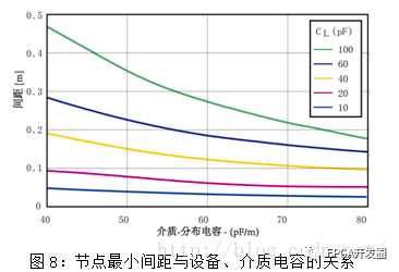
Equation 4 shows that the minimum spacing between devices is a function of distributed media and load capacitance, and Figure 8 illustrates their graphical relationship.
The load capacitance includes: bus pin wires, connectors, PCB traces, protective devices, and any physical wiring connected to the trunk. Therefore, the electrical distance from the transceiver to the bus trunk should be kept as short as possible.
Typical 5V transceivers have a capacitance of 7pF, while 3.3V transceivers double this to approximately 16pF. PCB traces add about 0.5 to 0.8pF of capacitance per centimeter, depending on the material and structure of the PCB, while the capacitance values for connectors and protective devices (such as surge protection circuits) can vary widely. The distributed capacitance of unshielded twisted pair media is approximately 40pF/m to 70pF/m.
When designing a remote data link, designers must assume significant ground potential differences (GPD) exist. These voltages (Vn) can superimpose as common-mode interference on the transmission line. If the superimposed interference signal exceeds the receiver’s input common-mode range, relying on local grounding as a current return path is very dangerous, as shown in Figure 9a.
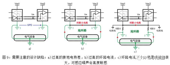
Since remote nodes are likely powered by electrical devices in different regions, servicing these devices can cause ground potential differences to exceed the receiver’s input common-mode range. Thus, a data link that works today may stop functioning at some point in the future.
Connecting directly to the remote ground via a grounding wire is also not recommended, as shown in Figure 9b. This is because large loop ground currents can introduce common-mode noise onto the signal lines.
The RS-485 standard recommends isolating these two grounds by inserting a resistor between the device ground and the system ground, as shown in Figure 9c. Although this method reduces loop currents, the presence of large loop grounds still makes the data link sensitive to noise generated somewhere along the loop.
A method for establishing a robust RS-485 data link capable of tolerating thousands of volts of ground potential difference while allowing long-distance transmission is signal and power supply isolation, as shown in Figure 10.
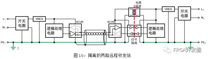
In this case, power isolation (DC/DC isolation) and signal isolation (optocouplers) can prevent current flow between remote system grounds and avoid the generation of loop currents.
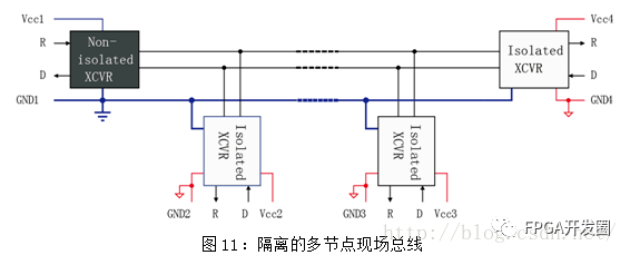
However, Figure 10 shows only two isolated transceiver nodes, while Figure 11 provides an example of isolated transceivers in a multi-node setup. Except for a non-isolated transceiver that provides a single reference ground, all other transceivers connect to the bus through isolation.
This design report covers the main aspects of RS-485 system design. Although there is a vast technical literature available on this topic, the purpose of this document is to provide a systematic design guide for engineers unfamiliar with RS-485.
The reference documents below provide detailed application reports that can help you complete a robust RS-485 compatible system design in a short time.
Texas Instruments (TI) offers a wide range of RS-485 transceiver products, including low EMI, low power (1/8 UL), high ESD protection (from 16kV to 30kV), and integrated failsafe features to address issues arising from open circuits, short circuits, and idle buses. For long-distance applications requiring isolation, TI also has corresponding products that provide unidirectional and bidirectional digital signal isolation at various rates and DC/DC power isolation.
Testing 5G UFMC Signal Modulation Transmission Standards Based on NI SDR and PXI Platform
[Expert Q&A] PetaLinux PSS_REF_CLK Binding Issues
Converting Floating Point to Fixed Point to Significantly Reduce Power Consumption and Costs
[Expert Q&A] MIG 7 Series Timing Analysis — Alarms on DQS Pins — Input Delay Constraint Loss
Bittware Application of Xilinx Virtex UltraScale+ VU13P to Expand XUPVV4 PCIe Card
Massive MIMO and Beamforming: Signal Processing Behind the 5G Buzzwords
Modern Heavy Industries Use NI HIL (Hardware-in-the-Loop) Simulation to Accelerate Product Development
Xilinx Fully Programmable Devices: Excellent Development Platform for Compute-Intensive Systems
Will Neural Networks Become the Future Trend of Machine Vision?
Solving Autonomous Driving Data Processing and Transmission Challenges, Zynq Platform Emerges
Where the Heart Leads, All Roads Lead There — “Post-90s” Fully Programmable Innovation Forces Shine at DDC 2017 China Finals
Intelligent and Efficient: Adaptive Building Models
Wow! Zynq Reduces Hybrid Vehicle Nitrogen Oxide Emissions by 50%!
Baido Cloud FPGA Standard Development Environment
Must-See Content | Learning How to Obtain a Vivado License
Strong Attack, Baidu Deploys Xilinx FPGA on New Public Cloud Acceleration Service
HLS Video Tutorial 25: Course System Introduction and Summary
In the Era of Big Data, How to Leverage Both CPU and FPGA Advantages Simultaneously?

Scan the QR code to apply for group entry