Today, I will share a document from TI titled “RS-485 Design Guide”. Reply “485 Design Guide” in the public account backend to obtain the complete PDF.
1 Introduction
In 1983, the Electronic Industries Association (EIA) approved a new balanced transmission standard known as RS-485. It has been found that RS-485 is highly praised and is widely used in industrial, medical, and consumer products, becoming the main specification for industrial interfaces.
This application report provides a design guide for engineers who are not familiar with the RS-485 standard, helping them to complete robust and reliable data transmission designs in the shortest time possible.
This application report provides a design guide for engineers who are not familiar with the RS-485 standard, helping them to complete robust and reliable data transmission designs in the shortest time possible.
2 Standards and Features
RS-485 is merely an electrical standard. Unlike complete interface standards that define functional, mechanical, and electrical specifications, RS-485 only defines the electrical characteristics of drivers and receivers using balanced multipoint transmission lines.
However, many higher-level standards specify RS-485 as a reference standard, such as China’s electric meter communication protocol standard DL/T645, which explicitly designates RS-485 as the physical layer standard.
The main features of RS-485 are:
•Multipoint with a Single 5V Power Supply
•-7V to +12V Bus Common Mode Range
•10Mbps Maximum Data Rate (Distance of 40 Feet)
•4000 Feet Maximum Cable Length (Rate of 100kbps)
The RS-485 standard recommends using a daisy chain to connect its nodes, also known as shared line or bus topology (see Figure 3-1). In this topology, the drivers, receivers, and transceivers used are connected to the backbone line via short network stubs. The interface bus can be designed for full-duplex or half-duplex transmission (see Figure 3-2).
Full-duplex requires two signal pairs (four wires) and a full-duplex transceiver, which has separate bus access lines for the transmitter and receiver. Full-duplex mode allows nodes to send data on one pair while receiving data on the other.
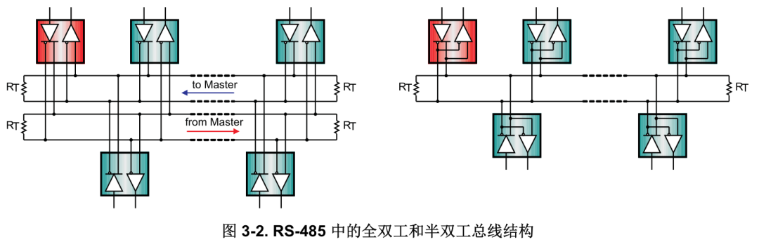
In half-duplex mode, only one pair of signals is used, and it requires driving and receiving data at different times. Both implementations require direction control signals (e.g., driver/receiver enable signals) to control all nodes, ensuring that at any time, only one driver is active on the bus. Multiple drivers accessing the bus simultaneously can lead to bus contention, which must be avoided through software control at all times.
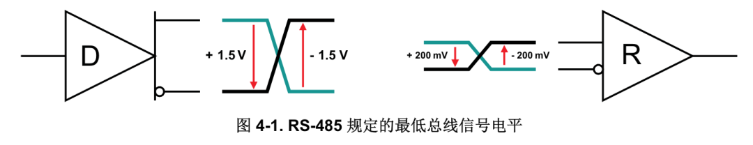
Drivers compliant with the RS-485 standard can provide a differential output of no less than 1.5V on a 54Ω load, while receivers compliant with the standard can detect differential inputs as low as 200mV. Even under severe signal attenuation from cables and connectors, these two values still provide ample margin for high-reliability data transmission. This robustness is the main reason why RS-485 is well-suited for long-distance networking in noisy environments.
Transmitting differential signals over twisted pairs is advantageous for RS-485 applications because external interference sources couple equally to both signal wires in a common mode, and this noise is filtered out by the differential receiver.
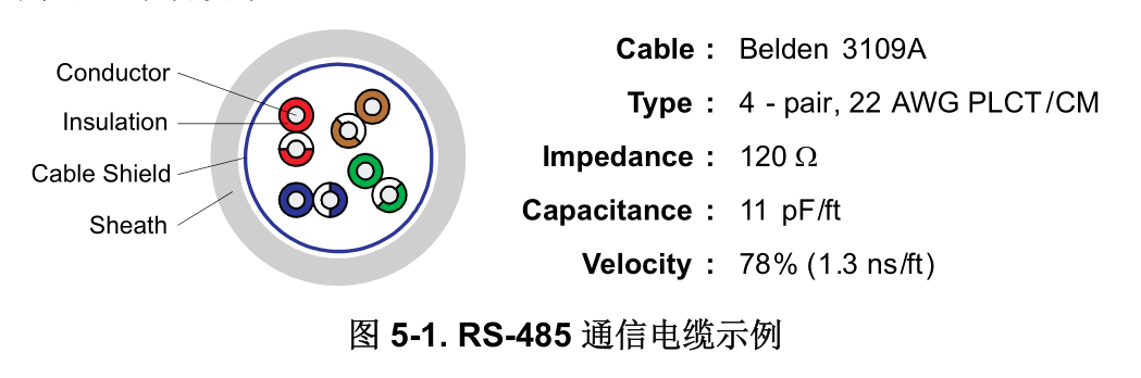
Industrial RS-485 cables are divided into shielded, unshielded, twisted pairs, and unshielded twisted pairs, complying with 22-24AWG wire gauge, with a characteristic impedance of 120Ω. Figure 5-1 shows the cross-section of a four-wire pair cable, which is typically used for two full-duplex networks. Similar cables with two pairs and single pairs can be used for low-cost half-duplex system designs.
In addition to network wiring, the RS-485 standard mandates that the printed circuit board layout and connectors of devices must be consistent with the electrical characteristics of the network, which can be achieved by keeping the two signal lines on the printed circuit board as close and equal in length as possible.
6 Bus Termination and Stub Lengths
To avoid signal reflections, data transmission lines should always be terminated, and stubs should be kept as short as possible. Proper termination requires matching the terminal resistor RT with the characteristic impedance Z0 of the transmission cable. The RS-485 standard recommends using a cable with Z0 = 120Ω, so the cable trunk is usually terminated with 120Ω resistors, one at each end of the cable (see the left half of Figure 6-1).
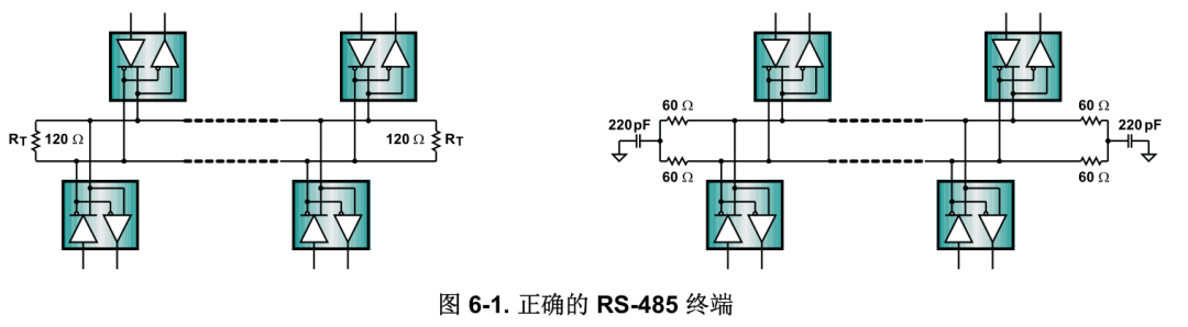
In noisy environments, the 120Ω resistors are typically replaced with two 60Ω resistors to form a low-pass filter, providing additional common mode noise filtering capability (see the right half of Figure 6-1). It is essential to match the resistor values (preferably using resistors with 1% accuracy) to ensure that both filters have the same frequency roll-off. A larger resistor tolerance (i.e., 20%) can result in different cut-off frequencies for the filters, and common mode noise can convert to differential noise, reducing the receiver’s immunity to interference.
The electrical length of the stub (the distance between the transceiver and the cable trunk) should be less than 1/10 of the driver output rise time and can be derived using the following formula:
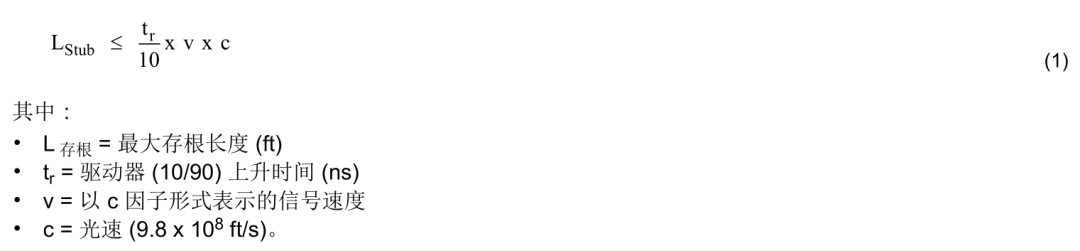
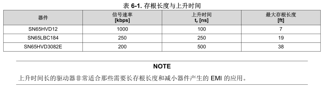
Table 6-1 lists the maximum stub lengths corresponding to the rise times of various drivers shown in Figure 5-1 (at 78% rate).
Failure protection enables the receiver to output a defined state in the absence of an input signal.
There are three possible causes for a loss of signal (LOS):
1.Open Circuit: Cable break or transceiver disconnected from the bus
2.Short Circuit: Wires in the differential pair touch each other due to insulation failure
3.Bus Idle: This occurs when all bus drivers are inactive.
Under the above conditions, when the input signal is zero, traditional receivers output a random state. Modern transceivers include a bias circuit that can protect against open circuits, short circuits, and bus idle conditions, ensuring that the receiver can force a defined state even when the signal is lost.
The downside of these failure protection designs is that the worst-case noise margin is only 10mV, so in noisy environments, external failure protection circuits should be added to increase the noise margin.
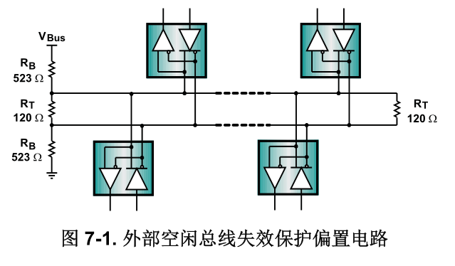
External failure protection circuits consist of a resistor voltage divider that can generate sufficient bus differential voltage to drive the receiver to produce a defined output state. To ensure adequate noise margin, in addition to the 200mV receiver input threshold, VAB must also include the measured maximum differential noise, VAB = 200mV + V_noise.

The minimum bus voltage is 4.75V, (5V – 5%), VAB = 0.25V, and Z0 = 120Ω, then RB is 528Ω. Inserting two 523Ω series resistors into RT establishes the failure protection circuit shown in Figure 7-1.
The output of the driver depends on the current it must provide to the load, so adding transceivers and failure protection circuits increases the total load current required on the bus. To estimate the maximum possible bus load number, RS-485 specifies a unit load (UL) assumption, which represents approximately 12kΩ of load impedance. Compliant drivers must be able to drive up to 32 of these unit loads. Modern transceivers often reduce the unit load to, for example, 1/8 UL, allowing up to 256 transceivers to be connected on the bus.
The failure protection bias can contribute up to 20 unit loads to the total bus load, so the maximum number of transceivers N is reduced to:
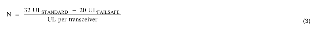
Therefore, when using 1/8-UL transceivers, up to 96 devices can be connected to the bus.
9 Data Rate and Bus Length
At a given data rate, the maximum bus length is limited by transmission line losses and signal jitter. When the jitter of the baud period is 10% or more, data reliability drops sharply. Figure 9-1 shows the relationship curve between the cable length and data rate for traditional RS-485 cables under 10% signal jitter.
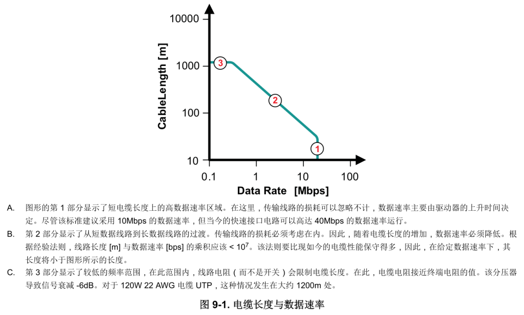
The RS-485 bus is a distributed parameter circuit, and its electrical characteristics are primarily determined by the inductance and capacitance distributed along the physical medium (including interconnecting cables and printed circuit board traces).
Adding capacitance to the bus in the form of devices and their interconnections reduces the bus impedance and leads to impedance mismatches in the medium and load portions of the bus. When input signals reach these locations, some are reflected back to the signal source, causing distortion of the driver output signal.
To ensure that the voltage level of the first signal transmitted from the driver remains valid at the receiver input, the minimum load impedance anywhere on the bus must be Z’> 0.4 x Z0, which can be achieved by maintaining a minimum distance d between bus nodes:

Where CL is the lumped load capacitance, and C is the capacitance per unit length of the medium (cable or PCB trace).
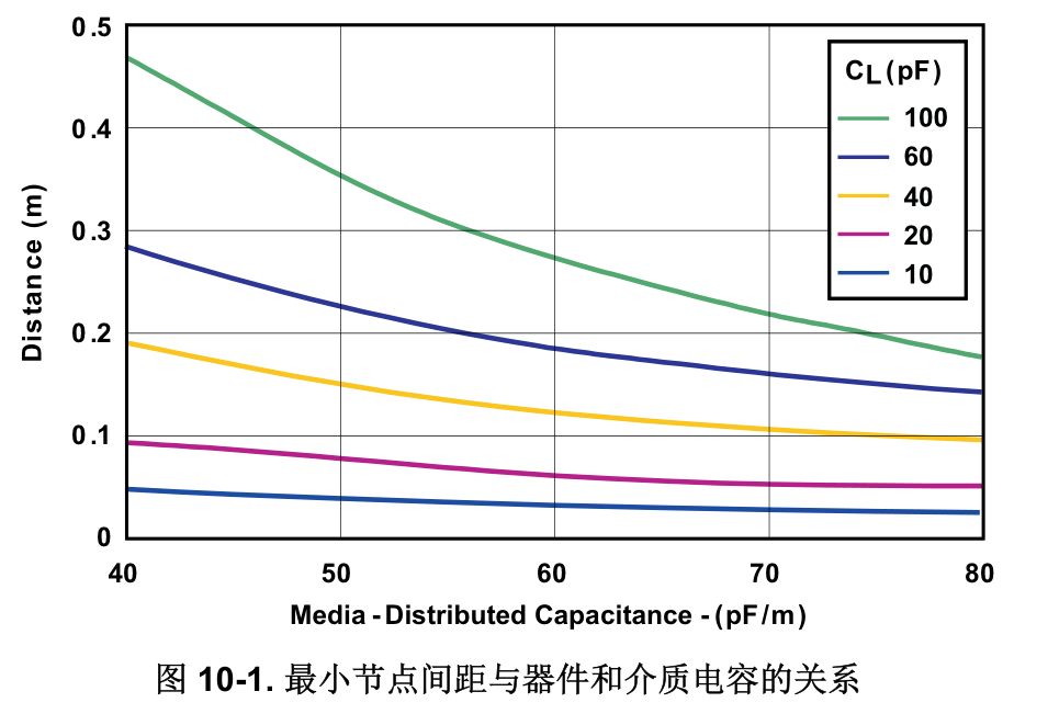
Equation 4 shows the function relationship between the minimum device spacing and the distributed and lumped load capacitances; Figure 10-1 graphically illustrates this relationship.
The load capacitance comes from the bus pin, connector contacts, printed circuit board traces, protective devices, and any other physical connections to the trunk. Therefore, the electrical distance from the bus to the transceiver (stub area) should be kept as short as possible.
The following discusses the capacitance values of various components:
The capacitance of a 5V transceiver is typically 7pF, while that of a 3V transceiver is about twice that of a 5V transceiver. PCB traces vary in structure, adding approximately 0.5~0.8pF capacitance per centimeter. The capacitance of connectors and suppression devices can vary widely. The distributed capacitance of the medium ranges from 40pF/m (low-capacitance unshielded twisted pair cable) to 70pF/m (backplane).
11 Grounding and Isolation
When designing remote data links, designers must assume significant ground potential differences (GPD). These voltages Vn will superimpose as common-mode interference on the transmission line. Even if the total superimposed signals are within the common-mode range at the receiver input, relying on local grounding as a reliable current return path can be very dangerous (see Figure 11-1a).
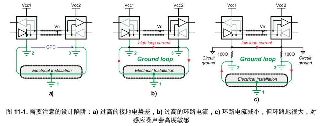
Since remote nodes may draw power from different parts of the electrical device, modifications to such devices (i.e., during maintenance) can cause the ground potential difference to exceed the common-mode range at the receiver input. Therefore, a data link that works normally today may stop functioning at some point in the future.
It is also recommended not to connect the remote ground directly via a ground wire (see Figure 11-1b), as large loop ground currents can introduce common-mode noise onto the signal lines.
To connect the remote ground directly, the RS485 standard recommends isolating the device ground from the local system ground by inserting resistors (see Figure 11-1c). Although this method reduces loop currents, the presence of large loop grounds still makes the data link sensitive to noise generated somewhere along the loop.
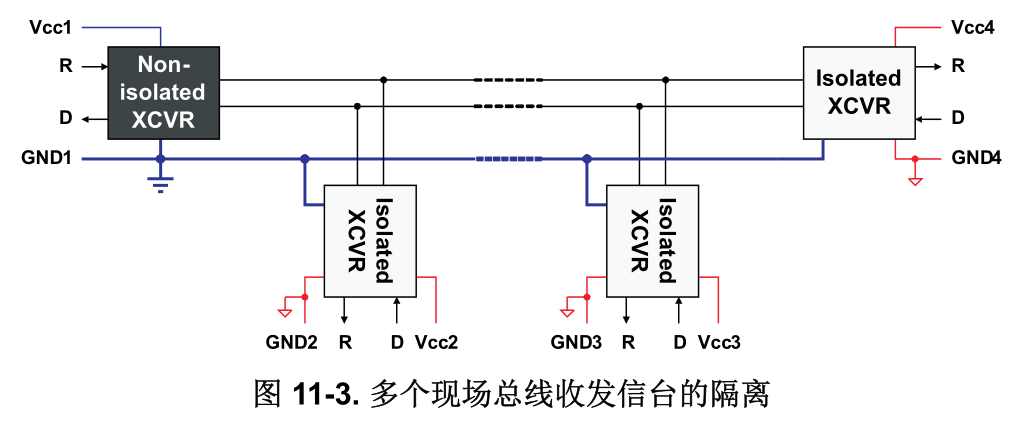
A robust RS-485 data link method that can tolerate thousands of volts of ground potential difference and transmit over long distances is signal and power supply isolation (see Figure 11-2).
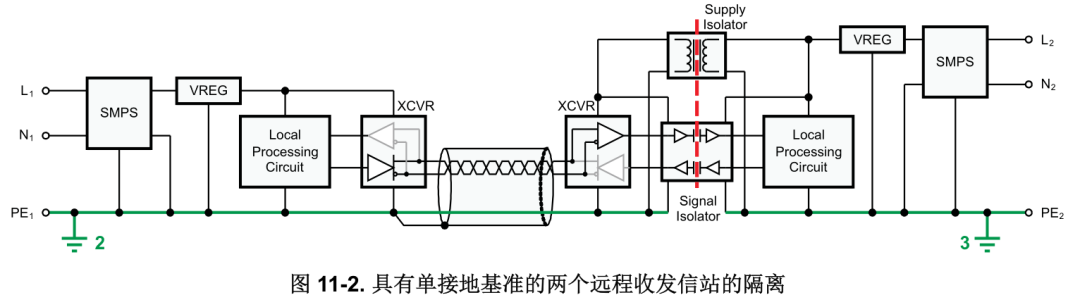
In this case, power isolators (such as isolated DC-DC converters) and signal isolators (such as digital capacitive isolators) can prevent current from flowing between remote system grounds and avoid generating loop currents.
Figure 11-2 shows the detailed connection of two transceiver nodes, while Figure 11-3 provides examples of multiple isolated transceivers. Except for one transceiver, all transceivers are connected to the bus via isolation. The non-isolated transceiver on the left provides a single ground reference for the entire bus.
This account maintains neutrality regarding all original and reprinted articles, and the articles pushed are for readers’ learning and communication purposes only. The rights to the articles, images, etc., belong to the original authors. If there is any infringement, please contact us for deletion.
Analysis and Debugging of RJ45 Circuit EMC Issues Column (II)
Buck DC-DC EMC Problem Debugging Ideas and Techniques
Why Can’t You Use LDO Well?
Share 💬 Like 👍 Read ❤️
Support quality content with a “three-click” action!
Every little bit counts, keep learning
Get more valuable content