Today, I would like to share a document from TI titled “RS-485 Design Guide”, which can serve as an introduction. The document link is as follows:
https://www.ti.com.cn/cn/lit/pdf/zhcaa89
1 Introduction
In 1983, the Electronic Industries Association (EIA) approved a new balanced transmission standard known as RS-485. It was found that RS-485 was highly praised and widely used in industrial, medical, and consumer products, becoming a major specification for industrial interfaces.
This application report provides design guidelines for engineers who are unfamiliar with the RS-485 standard, helping them to complete robust and reliable data transmission designs in the shortest time.
This application report provides design guidelines for engineers who are unfamiliar with the RS-485 standard, helping them to complete robust and reliable data transmission designs in the shortest time.
2 Standards and Features
RS-485 is merely an electrical standard. Compared to complete interface standards that define functional, mechanical, and electrical specifications, RS-485 only defines the electrical characteristics of drivers and receivers using balanced multipoint transmission lines.
However, many higher-level standards reference RS-485 as a standard, such as China’s electric meter communication protocol standard DL/T645, which explicitly specifies RS-485 as the physical layer standard.
The main features of RS-485 are:
•Multipoint with a single 5V power supply
•–7V to +12V bus common mode range
•10Mbps maximum data rate (distance of 40 feet)
•4000 feet maximum cable length (at a rate of 100kbps)
The RS-485 standard recommends using a daisy chain to connect its nodes, also known as shared line or bus topology (see Fig. 3-1). In this topology, the drivers, receivers, and transceivers used are connected to the trunk line via short stubs. The interface bus can be designed for full-duplex or half-duplex transmission (see Fig. 3-2).
Full-duplex implementation requires two pairs of signals (four wires) and a full-duplex transceiver, which has separate bus access lines for the transmitter and receiver. Full-duplex mode allows nodes to send data on one pair while receiving data on the other pair.
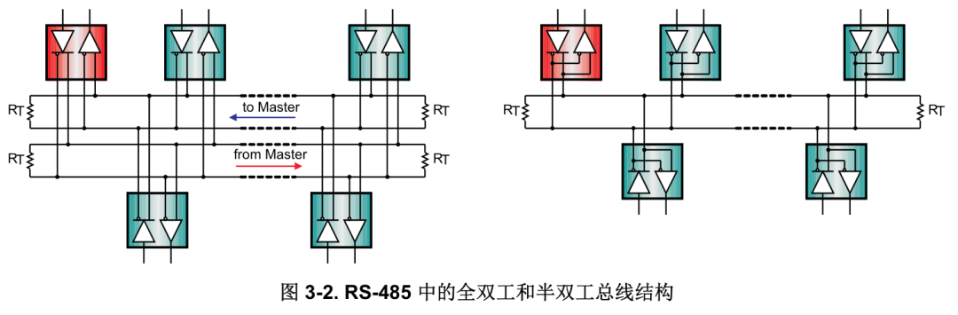
In half-duplex mode, only one pair of signals is used, requiring data to be driven and received at different times. Both implementations require direction control signals (such as driver/receiver enable signals) to control all nodes, ensuring that only one driver is active on the bus at any time. Multiple drivers accessing the bus simultaneously will cause bus contention, which must be avoided through software control at all times.
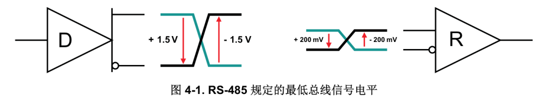
Drivers compliant with the RS-485 standard can provide a differential output of no less than 1.5V on a 54Ω load, while receivers compliant with the standard can detect differential inputs as low as 200mV. Even in cases where the signal is severely attenuated by cables and connectors, these values still provide sufficient margin for reliable data transmission. This robustness is a key reason why RS-485 is very suitable for long-distance networking in noisy environments.
Transmitting differential signals over twisted pairs is beneficial for RS-485 applications, as external interference sources couple equally to both signal lines in a common mode, and this noise is filtered out by the differential receiver.
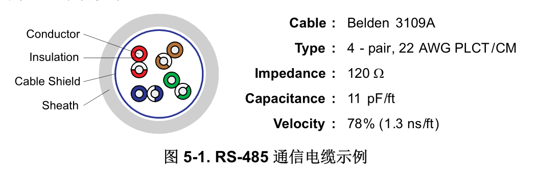
Industrial RS-485 cables are categorized into shielded, unshielded, twisted pairs, and unshielded twisted pairs, with cables conforming to 22-24AWG wire gauge having a characteristic impedance of 120Ω. Fig. 5-1 shows the cross-section of a four-wire pair cable, which is commonly used for two full-duplex networks. Similar cables with two pairs and single pair versions can be used for low-cost half-duplex system designs.
In addition to network wiring, the RS-485 standard mandates that the PCB layout and connectors of devices be consistent with the electrical characteristics of the network, which can be achieved by keeping the two signal lines on the PCB as close and equal in length as possible.
6 Bus Termination and Stub Length
To avoid signal reflections, the data transmission line should always be terminated, and the stubs should be as short as possible. Proper termination requires the terminal resistance RT to match the characteristic impedance Z0 of the transmission cable. The RS-485 standard recommends using cables with Z0 = 120Ω, so the cable trunk is typically terminated with 120Ω resistors at both ends (see the left part of Fig. 6-1).
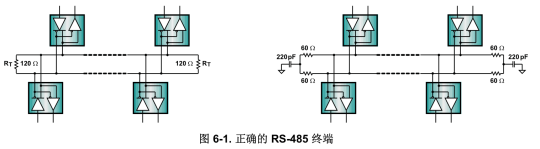
In applications in noisy environments, the 120Ω resistors are often replaced with two 60Ω resistors to form a low-pass filter, providing additional common-mode noise filtering capability (see the right part of Fig. 6-1). It is essential to match resistor values (preferably using 1% tolerance resistors) to ensure that both filters have equal frequency roll-off. A larger resistor tolerance (i.e., 20%) will result in different cutoff frequencies for the filters, and common-mode noise will convert to differential noise, thus reducing the receiver’s immunity to interference.
The electrical length of the stub (the distance between the transceiver and the cable trunk) should be less than 1/10 of the driver output rise time and can be derived using the following formula:
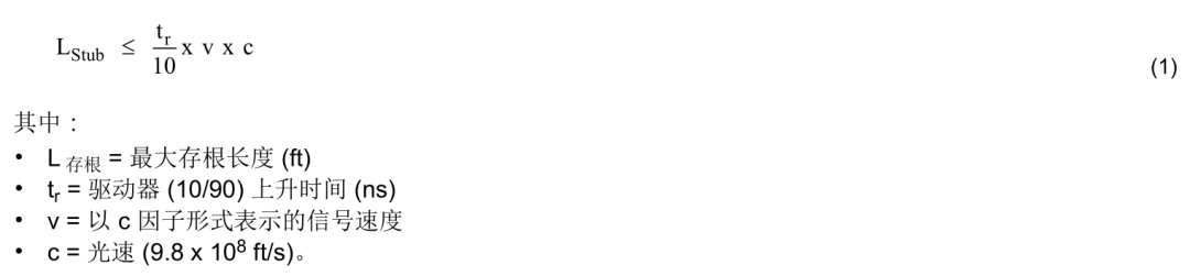
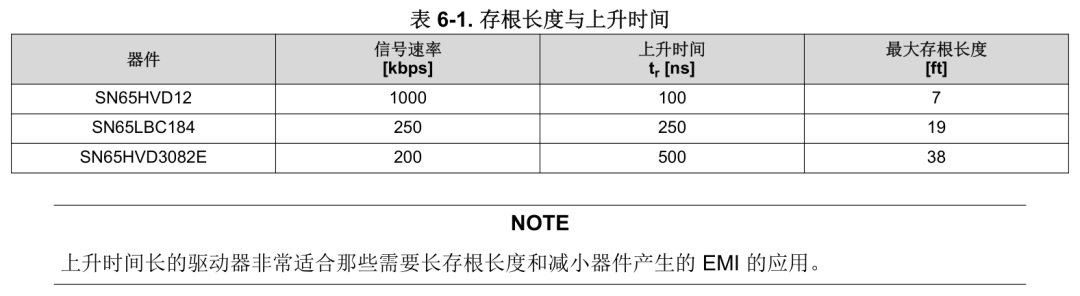
Table 6-1 lists the maximum stub lengths corresponding to the rise times of various drivers at a rate of 78% in Fig. 5-1.
Failure protection enables the receiver to output a defined state in the absence of an input signal.
There are three possible causes for loss of signal (LOS):
1.Open Circuit: Cable interruption or transceiver disconnection from the bus
2.Short Circuit: The wires of the differential pair come into contact due to insulation failure
3.Bus Idle: This occurs when all bus drivers are inactive.
Under the above conditions, when the input signal is zero, traditional receivers will output a random state. Modern transceivers include a bias circuit that can protect against open circuits, short circuits, and bus idle, allowing the receiver to force an output of a defined state even when the signal is lost.
The downside of these failure protection designs is that the worst-case noise tolerance is only 10mV. Therefore, in noisy environments, external failure protection circuits should be added to increase noise tolerance.
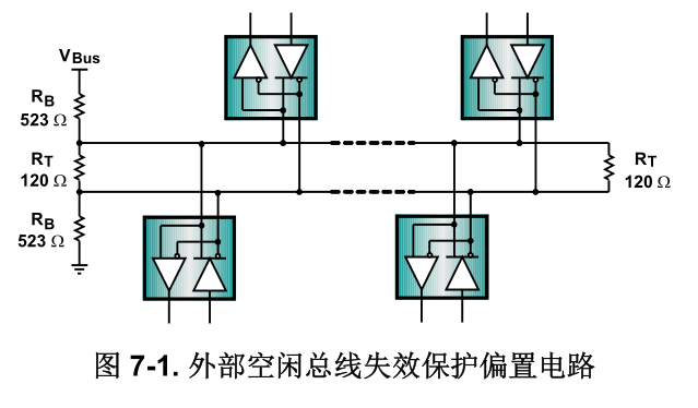
The external failure protection circuit consists of a resistor divider that can produce sufficient differential voltage to drive the receiver to produce a defined output state. To ensure sufficient noise tolerance, in addition to the 200mV receiver input threshold, VAB must also include the measured maximum differential noise, VAB = 200mV + V noise.

The minimum bus voltage is 4.75V, (5V – 5%), VAB = 0.25V, and Z0 = 120Ω, thus RB is 528Ω. Inserting two 523Ω series resistors into RT will establish the failure protection circuit shown in Fig. 7-1.
The output of the driver depends on the current it must provide to the load; thus, adding transceivers and failure protection circuits to the bus increases the required total load current. To estimate the possible maximum bus load number, RS-485 specifies a hypothetical unit load (UL) that represents approximately 12kΩ of load resistance. Compliant drivers must be able to drive up to 32 of these unit loads. Currently used transceivers can often reduce the unit load, for example, 1/8 UL, allowing up to 256 transceivers to be connected to the bus.
The failure protection bias can contribute up to 20 unit loads to the total bus load, thus reducing the maximum number of transceivers N to:
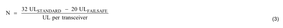
Therefore, when using 1/8-UL transceivers, up to 96 devices can be connected to the bus.
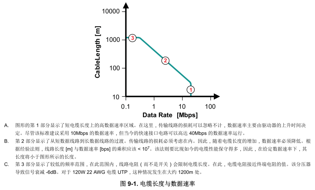
9 Data Rate and Bus Length
At a given data rate, the maximum bus length is limited by transmission line losses and signal jitter. When the jitter of the baud cycle is 10% or more, data reliability sharply decreases. Fig. 9-1 shows the relationship curve between cable length and data rate for traditional RS-485 cables under 10% signal jitter.
The RS-485 bus is a distributed parameter circuit, and its electrical characteristics are primarily determined by the inductance and capacitance distributed along the physical medium (including interconnecting cables and PCB traces).
Adding capacitance to the bus in the form of devices and their interconnections will lower the bus impedance and cause impedance mismatch in the medium and load portions of the bus. When the input signal reaches these points, some will reflect back to the signal source, causing distortion in the driver output signal.
To ensure that the first signal transmitted from the driver output remains valid at the receiver input, the minimum load impedance anywhere on the bus must be Z’ > 0.4 x Z0, which can be achieved by maintaining a minimum distance d between bus nodes:

where CL is the lumped load capacitance, and C is the distributed capacitance per unit length (cable or PCB trace).
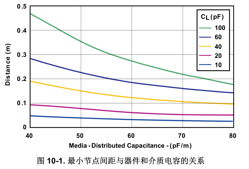
Equation 4 shows the functional relationship between the minimum device spacing and the distributed media and lumped load capacitance; Fig. 10-1 graphically illustrates this relationship.
The load capacitance comes from the bus pins of the line circuit, connector contacts, PCB traces, protective devices, and any other physical connections to the trunk. Therefore, the electrical distance from the bus to the transceiver (stub area) should be as short as possible.
The capacitance values of various capacitors are introduced below:
The capacitance of 5V transceivers is typically 7pF, while that of 3V transceivers is about twice that of 16pF. The capacitance of PCB traces varies depending on their structure, increasing by approximately 0.5~0.8pF per centimeter. The capacitance of connectors and suppressor devices can vary widely. The distributed capacitance of the medium ranges from 40pF/m (low-capacitance unshielded twisted pair cables) to 70pF/m (backplane).
11 Grounding and Isolation
When designing remote data links, designers must assume significant ground potential differences (GPD). These voltages Vn will superimpose on the transmission lines as common-mode interference. Even if the total superimposed signal is within the common mode range at the receiver input, relying on local grounding as a reliable current return loop is very dangerous (see Fig. 11-1a).
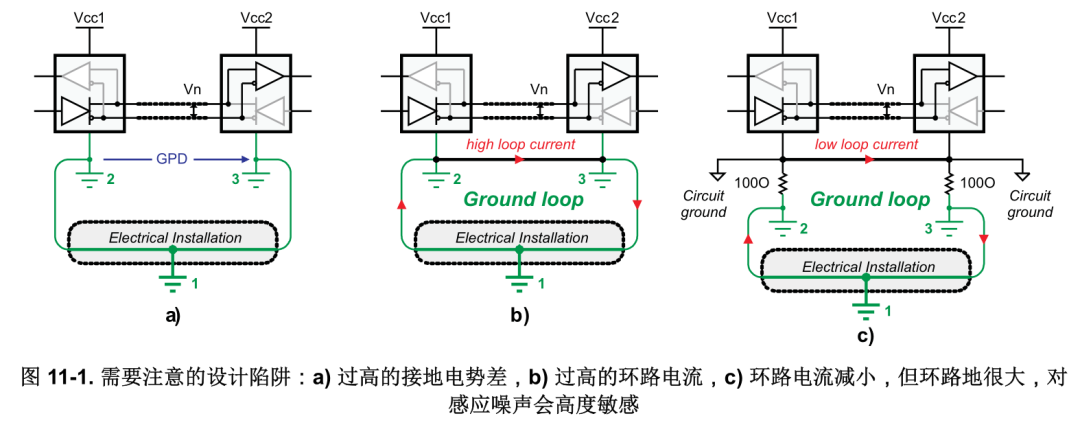
Since remote nodes may draw power from different parts of the electrical device, modifications to such devices (i.e., during maintenance work) may cause the ground potential difference to exceed the common mode range of the receiver input. Therefore, a data link that works fine today may stop functioning at some point in the future.
It is also recommended not to directly connect the remote ground via a ground wire (see Fig. 11-1b), as large loop ground currents can introduce common-mode noise onto the signal lines.
To connect the remote ground directly, the RS485 standard recommends isolating the device ground from the local system ground by inserting resistors (see Fig. 11-1c). Although this method reduces loop currents, the presence of large loop grounds still makes the data link sensitive to noise generated somewhere along the loop. Therefore, up to now, a robust data link has not been established.
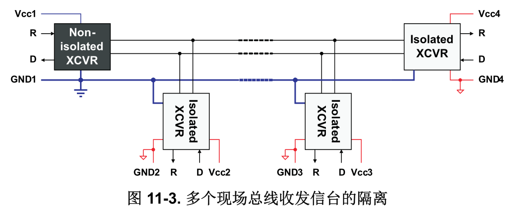
A method for establishing an RS-485 data link that can tolerate thousands of volts of ground potential difference and is robust for long-distance transmission is signal and power isolation (see Fig. 11-2).
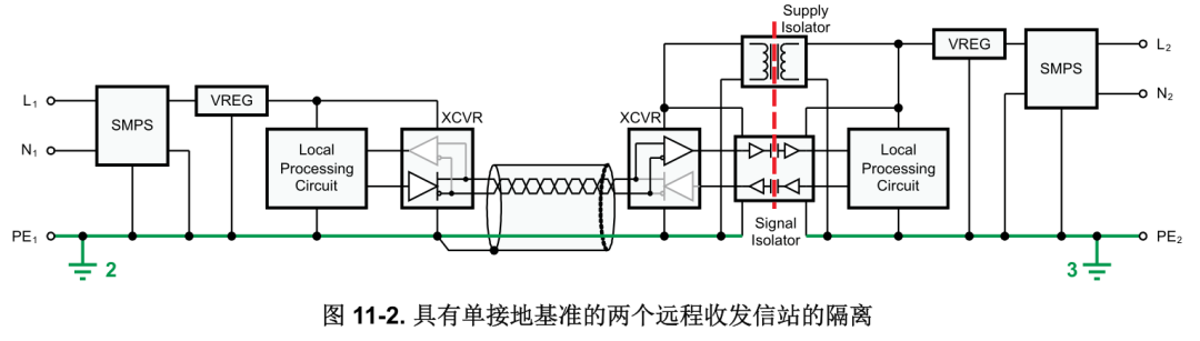
In this case, power isolators (such as isolated DC/DC converters) and signal isolators (such as digital capacitive isolators) can prevent current from flowing between remote systems’ grounds and avoid generating loop currents.
While Fig. 11-2 only shows the detailed connection of two transceiver nodes, Fig. 11-3 provides examples of multiple isolated transceivers. Except for one transceiver, all transceivers are connected to the bus through isolation. The non-isolated transceiver on the left provides a single ground reference for the entire bus.

Recommended Reading:
1、Still Using CAM350?
2、Everything I Wrote Is Here
3、Operational Amplifier 11 – Examples of Operational Amplifier Stability Assessment
4、Operational Amplifier -1 – Sources of Ideal Op-Amps and Virtual Short
5、The Ultimate Secrets of DCDC Layout