This series of articles will delve into the CDC issues, introducing CDC handling, CTS, and CDC timing constraints. If you’re interested, feel free to follow.The previous article 【Series】Detailed Explanation of Digital IC/FPGA Cross-Clock Domain Issues (4) Deep Understanding of Metastability (Part 2) introduced the probability of metastability and the estimation method for MTBF. This section will detail the “Asynchronous Reset and Synchronous Release” circuit.1. Principles of Asynchronous Reset/Synchronous ReleaseBefore introducing asynchronous reset/synchronous release, let’s first understand the drawbacks of synchronous reset and asynchronous reset.
- Synchronous Reset
- The DFF data input that is synthesized needs to be ANDed with the reset signal, consuming more logic resources;
- There is a requirement for the minimum pulse width of the reset signal, which must be greater than the clock period;
- Asynchronous Reset
- The reset signal is easily affected by glitches, and since the reset release process is asynchronous with the clock sampling edge, when the reset release time falls within the recovery_time and removal_time window, as discussed in 【Series】Detailed Explanation of Digital IC/FPGA Cross-Clock Domain Issues (3) Deep Understanding of Metastability (Part 1), the circuit is prone to metastability;
- Asynchronous Reset/Synchronous Release
-
The application of the reset process is not affected by the clock, meaning that as long as rst_n is low, the reset is effectively applied;
-
The reset release behavior is synchronized with the clock sampling edge, effectively avoiding metastability issues during the reset release process.
So, what are the advantages of asynchronous reset/synchronous release:
- The reset application process is independent of the clock sampling edge, and it can effectively capture short pulse resets;
- The reset release behavior is synchronized with the clock sampling edge, effectively avoiding metastability issues during the reset release process
Next, let’s look at how the asynchronous reset/synchronous release circuit ensures the capture of short pulse reset signals. Taking the following diagram as an example, rst_i is the input short pulse reset signal (hard reset), and rst_o is the output reset signal.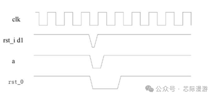
- Assuming rst_i_di (the reset signal applied to d1) is a short pulse with a width less than the clock period; since the reset release of d1 is synchronized with the clock edge, the output Q of d1 will have a pulse width (effective low time) greater than that of rst_i_di;
- Since d2 latches the output of d1, the output Q of d2 will further extend the pulse width (effective low time) by one clock cycle. Therefore, the final output reset signal (rst_o) is extended in width compared to the original hard reset input (rst_i).
How does the asynchronous reset/synchronous release circuit avoid metastability issues during the reset release process? We will discuss this by taking the case where the preceding and succeeding flip-flops cannot meet the reset recovery time requirements:
-
The preceding flip-flop cannot meet the recovery time requirement
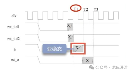
As shown in the figure, the preceding flip-flop does not meet the reset recovery time requirement, and its output a will exhibit metastability at the moment T1->T2. Similarly, at the moment T1->T2, d2 samples the value of a at T1, so the output of d2 remains 0. At the T2 sampling edge, the output of d1 will be in a stable state of either 0 or 1, thus the input to d2 at T2 is stable (effectively filtering out the metastability of d1).
-
The succeeding divider cannot meet the recovery time requirement
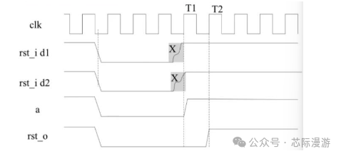
As shown in the figure, the preceding flip-flop meets the reset recovery time requirement, so the output a of d1 will release to 1 at T1; for the succeeding flip-flop d2, even if its reset does not meet the recovery time requirement, its input a and output state from T1 to T2 are determined, and at T2, it samples the already stable released a.
2. Implementation of Asynchronous Reset/Synchronous ReleaseHaving discussed the benefits of asynchronous reset/synchronous release, we also provide its corresponding RTL source code (very simple). The following diagram is the corresponding circuit diagram.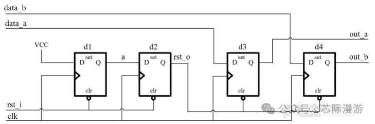 【Note】: The reset signal processed by asynchronous reset/synchronous release in the code is output by d2.
- 1
- 2
- 3
- 4
- 5
- 6
- 7
- 8
- 9
- 10
- 11
- 12
- 13
- 14
- 15
- 16
- 17
- 18
- 19
- 20
- 21
- 22
- 23
- 24
- 25
- 26
- 27
- 28
- 29
- 30
- 31
- 32
- 33
- 34
- 35
- 36
- 37
- 38
- 39
- 40
- 41
- 42
module sync_async_reset (
input    clk,
input    rst_i,
input    data_a,
input    data_b,
output   out_a,
output   out_b
 );

reg     d1, d2;
reg     d3, d4;
assign  out_a = d3;
assign  out_b = d4;
assign  rst_o = d2;

always @ (posedge clock, negedge rst_i) begin
if (!rst_i) begin
            d1 <= 1'b0;
end
elsebegin
            d1 <= 1'b1;
end
end
always @(posedge clock, negedge rst_i) begin
if(irst_i) begin
            d2 <= 1'b0;
end
elsebegin
            d2 <= d1;
end
end
always @ (posedge clock, negedge rst_o) begin
if (!rst_o) begin
            d3 <= 1'b0;
            d4 <= 1'b0;
end
elsebegin
            d3 <= data_a;
            d4 <= data_b;
end
end
endmodule
In the next article, we will delve into cross-clock domain processing methods. Stay tuned to Chip Journey public account for more digital IC/FPGA learning materials and autumn recruitment information.Previous highlights:【Series】Digital ASIC Design Confessions on Process Evaluation (1) PDK Evaluation Criteria and Precautions【Series】Detailed Explanation of Digital IC/FPGA Cross-Clock Domain Issues (4) Deep Understanding of Metastability (Part 2)【Series】Detailed Explanation of Digital IC/FPGA Cross-Clock Domain Issues (3) Deep Understanding of Metastability (Part 1)【Series】Detailed Explanation of Digital IC/FPGA Cross-Clock Domain Issues (2) Deep Understanding of Metastability (Part 1)【Series】Detailed Explanation of Digital IC/FPGA Cross-Clock Domain Issues (1) Synchronous and Asynchronous Clocks