A high-quality article on RS-485 design written by a TI engineer (2008), highly recommended for reading.
0. Introduction
Approved as a balanced transmission standard in the early 1980s (1983, Electronic Industries Alliance EIA), RS-485 seems to have become an everlasting interface standard in the industry. There is a wealth of literature on it, but for system engineers who have little exposure to interface design, such a vast amount of literature can be overwhelming.
This article aims to discuss the main content of the RS-485 standard and provide a beginner’s guide for designers who are new to it.
1. Standards and Features
RS-485 is merely an electrical standard. Unlike complete interface standards that define functional, mechanical, and electrical specifications, RS-485 only defines the electrical characteristics of drivers and receivers using balanced multipoint transmission lines.
However, many higher-level standards reference RS-485 as a standard, such as China’s electric meter communication protocol standard <span>DL/T645</span>, which explicitly specifies RS-485 as the physical layer standard.
The main features of RS-485 include:
- Balanced interface
- Multipoint using a single 5V power supply
- –7V to +12V common mode range
- Up to 32 unit loads
- 10Mbps maximum data rate (at a distance of 40 feet)
- 4000 feet maximum cable length (at a rate of 100kbps)
2. Network Topology
The RS-485 standard recommends using a daisy chain to connect its nodes, also known as shared line or bus topology (see Figure 1), where each node is connected to the main cable via short wire segments. This interface bus is typically designed for half-duplex transmission, meaning it uses only one pair of signal lines, and data driving and receiving can only appear on the signal line at different times.
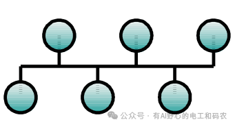
Figure 1: RS-485 Bus Structure
This requires a protocol to control node operations through direction control signals (e.g., driver/receiver enable signals) to ensure that only one driver is active on the bus at any time, avoiding multiple drivers accessing the bus simultaneously, which could lead to bus contention.
RS-485 can also achieve full duplex, which requires two pairs of signals (four wires) and full duplex transceivers that have separate bus access lines for transmitters and receivers.
Full duplex mode allows nodes to send data on one pair while receiving data on another pair.
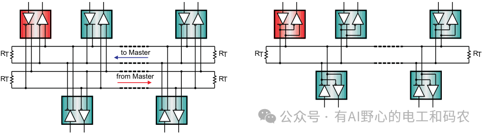
Figure 2: Full Duplex and Half Duplex Bus Structures in RS-485
3. Signal Levels
RS-485 drivers must provide a minimum differential output of 1.5V on a 54Ω load, while compliant RS-485 receivers must be able to detect a minimum differential input of 200mV (see Figure 2). These two values provide sufficient margin for reliable data transmission, even when signals experience significant attenuation through cables and connectors. Robustness is the main reason RS-485 is suitable for long-distance networking in noisy environments.

Figure 3: Minimum Bus Signal Levels Specified by RS-485
4. Cable Types
Transmitting differential signals over twisted pairs brings significant benefits to RS-485 applications. This is because noise from external sources is always equally coupled into both signal lines, which is common mode noise, and can be suppressed at the input of the differential receiver.
Industrial RS-485 cables are categorized into shielded, unshielded, twisted pairs, and unshielded twisted pairs, with cables conforming to 22-24AWG having a characteristic impedance of <span>120Ω</span>.
Figure 4 shows a cross-section of a four-pair cable, which is typically used for two full-duplex networks. Similar cables in two-pair and single-pair versions can be used for low-cost half-duplex system designs.
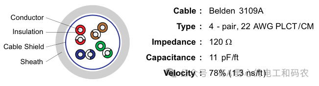
Figure 4: Example of RS-485 Communication Cable
To maintain the electrical characteristics of the network, in addition to the connections of the network cables, the RS-485 standard mandates that the printed circuit board layout and connectors of devices must be consistent with the electrical characteristics of the network, which can be achieved by keeping the two signal lines on the printed circuit board as close and equal in length as possible.
5. Bus Termination and Stub Length
To avoid signal reflections, data transmission lines should always be terminated, and stubs should be as short as possible. Proper termination requires matching the terminal resistance RT with the characteristic impedance Z0 of the transmission cable. The RS-485 standard recommends using a cable with <span>Z0 = 120Ω</span>, so the cable trunk is typically terminated with <span>120Ω</span> resistors, one at each end of the cable (see the left part of Figure 5).
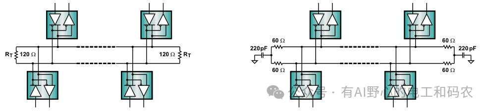
Figure 5: Correct RS-485 Termination
In noisy environments, applications often replace the <span>120Ω</span> resistors with two <span>60Ω</span> resistors, forming a low-pass filter to provide additional common mode noise filtering (see the right part of Figure 5). It is essential to match the resistor values (preferably using 1% tolerance resistors) to ensure that both filters have the same frequency roll-off. A larger resistor tolerance (i.e., <span>20%</span>) will result in different cutoff frequencies for the filters, and common mode noise will convert to differential noise, reducing the receiver’s immunity to interference.
The electrical length of the stub (i.e., the distance between the transceiver and the cable trunk) should be less than 1/10 of the driver output signal rise time, and can be derived from the following formula:

Where:
- Lstub = Maximum stub length (ft)
- tr = Driver (10/90) rise time (ns)
- v = Signal speed expressed in terms of c
- c = Speed of light (9.8 x 10^8 ft/s)
Table 1 lists the maximum stub lengths corresponding to various driver rise times at a rate of 78% shown in Figure 5.

Table 1: Stub Lengths and Unterminated Cable Lengths Under Different Signal Rise Times.
NOTE: Drivers with long rise times are very suitable for applications that require long stub lengths and reduced EMI generated by devices.
6. Failsafe
Failsafe refers to the ability of a receiver to guarantee a definite output state in the absence of an input signal.
There are three possible causes of signal loss (LOS):
- Circuit Open: Caused by a broken wire or a transceiver disconnected from the bus;
- Circuit Short: Caused by insulation failure leading to a short circuit between the two wires of the differential pair signal;
- Bus Idle: This occurs when all bus drivers are inactive.
Since the above conditions can cause traditional receivers to output random states when the input signal is zero, modern transceiver designs include dedicated bias circuits for failsafe operation under open, short, and bus idle conditions. When the input signal is zero, this circuit keeps the receiver’s output in a definite state.
Although these failsafe transceivers claim to reduce the number of components, their noise tolerance for failure protection is only 10mV, so in noisy environments, external failsafe circuits must be added to increase noise tolerance.
The external failsafe circuit includes a resistor divider to generate sufficient differential bus voltage to drive the receiver’s output to a definite state. To ensure the circuit has adequate noise margin, VAB must cover the maximum differential noise beyond the 200mV receiver input threshold.
The value of the failsafe bias resistor RB under worst-case conditions (i.e., minimum voltage, maximum noise conditions) can be calculated using the following formula:

Where VAB=200mV + VNoise. With a minimum bus voltage of 4.75V (i.e., 5V – 5%), VAB=0.25V and Zo=120, the calculated value of RB is 528Ω. By connecting two 523Ω resistors in series on RT, a failsafe circuit is established at one end of the bus (see the left part of Figure 6).
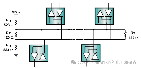
Figure 6: External Failsafe Bias for Bus Idle
7. Bus Loading
Since drivers rely on current output, a load must be provided for the output current. Adding transceivers and failsafe circuits to the bus also increases the total load current required. To estimate the maximum number of loads allowed on the bus, RS-485 defines a hypothetical unit load (UL), where one UL represents a load impedance of approximately 12kΩ. Compliant drivers must be able to drive <span>32</span> such unit loads. Modern transceivers often use reduced unit loads, such as <span>1/8UL</span>, allowing up to <span>256</span> transceivers to be connected to the bus.
Since the failsafe bias circuit can occupy up to 20UL of the bus load, the maximum number of receivers allowed on the bus is reduced. Therefore, when using 1/8UL transceivers, a maximum of 96 devices can be connected to the bus. That is:

8. Relationship Between Data Rate and Bus Length
The maximum bus length is limited by transmission line losses and signal jitter at a given data rate. When jitter reaches 10% or more of the baud period, data reliability drops sharply. Figure 7 shows the cable lengths corresponding to different data rates for traditional RS-485 drivers under 10% signal jitter.
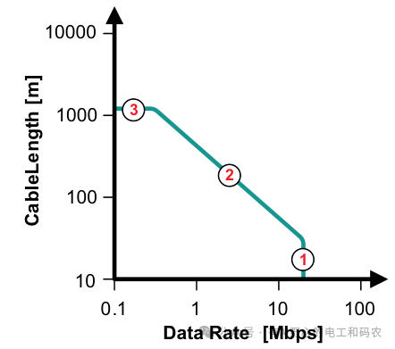
Figure 7: Cable Lengths at Different Data Rates
- The first part of the graph shows the high data rate region on short cable lengths. Here, the transmission line losses can be neglected, and the data rate is primarily determined by the driver’s rise time. Although the standard recommends a data rate of 10Mbps, today’s fast interface circuits can operate at data rates up to 40Mbps.
- The second part of the graph shows the transition from short data lines to long data lines. Transmission line losses must be taken into account. Therefore, as cable length increases, the data rate must decrease. According to the rule of thumb, the product of line length [m] and data rate [bps] should be < 107. This rule is much more conservative than today’s cable performance, so at a given data rate, its length will be less than what is shown in the graph.
- The third part shows the lower frequency range, where line resistance (rather than switching) limits cable length. Here, the cable resistance approaches the value of the termination resistance. This voltage divider causes a signal attenuation of -6dB. For 120Ω 22AWG UTP cable, this situation occurs at approximately 1200m.
9. Minimum Node Spacing
The RS-485 bus is a distributed parameter circuit, and its electrical characteristics are primarily determined by the inductance and capacitance distributed along the physical medium (including interconnecting cables and PCB traces).
Adding capacitance to the bus in the form of devices and their interconnections reduces the bus impedance and causes impedance mismatches between the medium and load portions of the bus. When the input signal reaches these locations, part of it reflects back to the signal source, causing distortion of the driver’s output signal.
To ensure that the first signal transmitted from the driver output remains valid at the receiver input, the minimum load impedance anywhere on the bus must satisfy Z’ > 0.4 x Z0, which can be achieved by maintaining a minimum distance d between bus nodes:

Where CL is the lumped load capacitance, and C is the medium capacitance per unit length (cable or PCB trace).
The above formula shows the functional relationship between minimum device spacing and distributed media and lumped load capacitance;
The following diagram graphically illustrates this relationship:
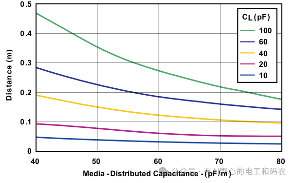
Figure 8: Relationship Between Minimum Node Spacing and Device and Medium Capacitance
Load capacitance comes from the bus pins, connector contacts, PCB traces, protection devices, and any other physical connections to the trunk. Therefore, the electrical distance from the bus to the transceiver (stub length) should be as short as possible.
The capacitance values of various components are as follows:
- 5V transceivers typically have a capacitance of 7pF, while 3V transceivers have about twice that capacitance of 16pF.
- PCB traces can add approximately 0.5~0.8pF capacitance per centimeter, depending on their structure.
- Capacitance from connectors and suppressor devices can vary widely.
- Medium distributed capacitance ranges from 40pF/m (low capacitance unshielded twisted pair cable) to 70pF/m (backplane).
10. Grounding and Isolation
Remote data connections often experience significant ground potential differences (GPD), which can become common mode noise at the transmitter’s output. If this noise is too high, it may exceed the input common mode noise tolerance of the receiver, potentially damaging the device. Even if the total superimposed signal is within the common mode range of the receiver input, relying on local grounding as a reliable return path for current is also risky. Therefore, relying on local grounding as a reliable return path for current is not recommended (see Figure 9a).
Since remote nodes may draw power from different parts of the electrical device, modifying such devices (i.e., during maintenance work) can cause the ground potential difference to exceed the input common mode range of the receiver. Thus, a data link that works fine today may stop functioning at some point in the future.
It is also not recommended to directly connect remote grounds (see Figure 9b), as this can lead to significant ground loop currents that couple into the data lines as common mode noise. As suggested by the RS-485 standard, inserting resistors in the grounding path to reduce loop currents only solves part of the problem. The presence of a large ground loop makes the data link very sensitive to noise generated elsewhere in the loop. Therefore, a reliable data link cannot be established in this manner (see Figure 9c).
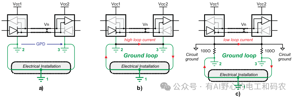
Figure 9: Design Flaws to Note: a) Excessive GPD; b) Excessive Loop Current; c) Reduced Loop Current, but Excessive Ground Loop Still Makes the Circuit Highly Sensitive to Induced Noise
A robust RS-485 data link method that can tolerate thousands of volts of ground potential difference and transmit over long distances is signal and power isolation (see Figure 10). When using this method, the signal and power lines of the bus transceivers are isolated from the local signals and power.
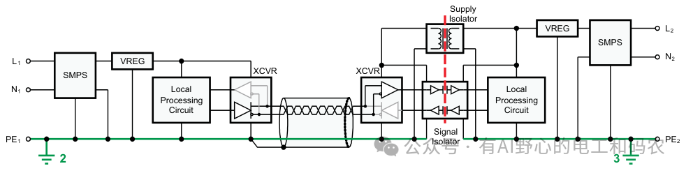
Figure 10: Isolation of Two Remote Transceiver Stations with a Single Ground Reference
In this case, signal isolators (e.g., digital capacitive isolators) and power isolators (e.g., isolated DC/DC converters) can prevent current from flowing between remote system grounds and avoid generating loop currents.
While Figure 10 only shows the detailed connections of two transceiver nodes, Figure 11 provides examples of multiple isolated transceivers. All transceivers except one are connected to the bus through isolation. The non-isolated transceiver on the left provides a single ground reference for the entire bus.
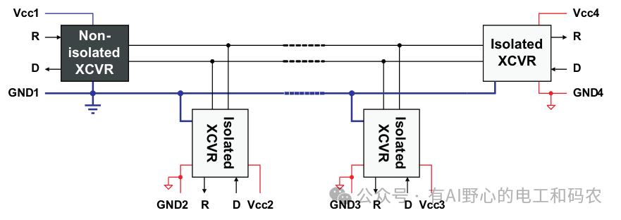
Figure 11: Isolation of Multiple Field Bus Transceiver Stations
11. Conclusion
The purpose of this application report is to highlight the key aspects of RS-485 system design. Despite the abundance of technical literature on this topic, the aim of this document is to provide a very comprehensive design guide for system designers unfamiliar with RS-485.
Following the procedures discussed in this document and consulting the detailed application reports in the references section can help you achieve a robust system design that meets RS-485 requirements in the shortest time possible.
To support design work, Texas Instruments (TI) offers a wide range of RS-485 transceiver products characterized by low EMI, low power (1/8UL), high ESD protection (from 16kV to 30kV), and integrated failure protection features for open, short, and idle bus conditions. For long-distance applications requiring isolation, unidirectional and bidirectional digital isolators (from DC to 150Mbps) in dual-channel, triple-channel, and quad-channel versions, as well as isolated DC/DC converters (with 3V and 5V regulated outputs), provide power through isolation barriers.
11.1 References
For more information, please visit www.ti.com and enter the following blue document numbers in the “keyword search” field.
- Eliminating Ground Noise in Data Transmission Systems Application Report (SLLA268)
- Interface Circuit Design Manual for TIA/EIA-485 (RS-485) (SLLA036)
- RS-485 Signal Loss Detection, TI Analog Applications Journal Q4 2006 (SLYT257)
- Overtemperature Protection in RS-485 Line Circuits Application Report (SLLA200)
- Device Spacing on RS-485 Bus, TI Analog Applications Journal Q2 2006 (SLYT241)
- PROFIBUS Electrical Layer Solutions Application Report (SLLA177)
- Common Mode Noise Statistical Survey, TI Analog Applications Journal November 2000 (SLYT153)
- Failure Protection in RS-485 Data Bus, TI Analog Applications Journal Q3 2004 (SLYT080)
- Limits on Unit Loads and Bus Connection Numbers on RS-485 Data Bus, TI Analog Applications Journal Q1 2004 (SLYT086)
- Using Signal Transmission Rates and Transmission Rates Application Report (SLLA098)
- RS-485 Transceivers Operating at Fast Signal Transmission Rates Application Report (SLLA173)
- RS-485 Application Report for Electric Meter Applications (SLLA112)
- Failure Protection in RS-485 Data Bus, TI Analog Applications Journal Q3 2004 (SLYT064)
- Using Receiver Equalization to Extend RS-485 Data Communication Application Report (SLLA169)
- Limits on Unit Loads and Bus Connection Numbers Application Report (SLLA166)
- Comparative Bus Solutions Application Report (SLLA067)
- RS-485 Application Report for Digital Motor Control (SLLA143)
- Overview and System Configuration of 422 and 485 Standards Application Report (SLLA070)
- Power and Speed Comparison of TIA/EIA-485 and M-LVDS Application Report (SLLA106)
- Field Insertion of Differential Interface Products Application Report (SLLA107)
- ISO72x Series High-Speed Digital Isolators Application Report (SLLA198)
Author: Thomas Kugelstadt
Senior Application Engineer
Texas Instruments, 2008