46 Basic Questions About FPGA You Should Know

1. What Are Setup and Hold Times?
Answer: Setup/Hold Time refers to the timing requirements between the input signal and the clock signal for testing chips.
Setup time is the time during which the data must remain stable before the rising edge of the clock signal arrives at the flip-flop. The input signal must arrive at the chip T time before the clock’s rising edge (if the rising edge is valid); this T is the setup time. If the setup time is not met, this data cannot be captured by the clock into the flip-flop; it can only be captured at the next clock’s rising edge.
Hold time is the time during which the data must remain stable after the clock signal’s rising edge has arrived. If the hold time is insufficient, the data also cannot be captured by the flip-flop.
2. What Are the Concepts of Race and Hazard? Solutions?
Answer: In combinational logic, when the input signal paths to a gate have different delays, resulting in inconsistent arrival times at that gate, it is called a race condition. The occurrence of glitches is called a hazard. If there are opposing signals in the Boolean expression, race and hazard phenomena may occur.
Solutions: One is to add a Boolean expression cancellation term, the second is to add capacitance externally to the chip, and the third is to add select signals. Excellent design solutions such as D flip-flops, Gray code counters, and synchronous circuits can eliminate these issues.
3. How to Solve Metastability?
Answer: Metastability refers to the inability of a flip-flop to reach a stable state within a specified time period. When a flip-flop enters a metastable state, its output level is unpredictable, and it is also uncertain when the output will stabilize at a correct level. During this unstable period, the flip-flop may output some intermediate levels or may oscillate, and this useless output can propagate through various flip-flops along the signal path.
Solutions:
1. Reduce the system clock frequency.
2. Use faster reacting flip-flops.
3. Introduce synchronization mechanisms to prevent metastability propagation.
4. Improve clock quality by using edge-fast clock signals; the key is to use better technology for devices and have a larger clock cycle margin.
4. Discuss the Advantages and Disadvantages of Static and Dynamic Timing Analysis.
Static timing analysis uses exhaustive analysis methods to extract all timing paths in the circuit, calculate the propagation delays of signals along these paths, and check whether the setup and hold times meet timing requirements. By analyzing the maximum and minimum path delays, errors that violate timing constraints can be identified. It does not require input vectors to exhaust all paths, and it runs quickly and occupies less memory. It can not only conduct comprehensive timing functional checks on chip designs but can also use the results of timing analysis to optimize the design. Therefore, static timing analysis has been increasingly used in the verification of digital integrated circuit design.
Dynamic timing simulation is the usual simulation; since it is impossible to generate complete test vectors that cover every path in the gate-level netlist, some timing issues that may exist on certain paths cannot be exposed in dynamic timing analysis.
Disadvantages of static timing analysis:
1. Cannot identify false paths.
2. Not suitable for asynchronous circuits.
3. Cannot verify functionality.
5. Write a piece of code in VERILOG to eliminate a glitch. The schematic to filter glitches shorter than one cycle is as follows:
46 Basic Questions About FPGA You Should Know
Verilog code implementation is as follows:
module digital_filter_(clk_in, rst, host_rst, host_rst_filter);
input clk_in;
input rst;
input host_rst;
output host_rst_filter;
reg host_rst_d1;
reg host_rst_d2;
always@(posedge clk_in or negedge rst)
begin
if(~rst)
begin
host_rst_d1 <= 1’b1;
host_rst_d2 <= 1’b1;
end
else
begin
host_rst_d1 <= host_rst;
host_rst_d2 <= host_rst_d1;
end
end
assign host_rst_filter = host_rst_d1 | host_rst_d2;
endmodule
The schematic to filter glitches longer than one cycle but less than two cycles is as follows:
46 Basic Questions About FPGA You Should Know
The Verilog code implementation is as follows:
module digital_filter_(clk_in, rst, host_rst, host_rst_filter);
input clk_in;
input rst;
input host_rst;
output host_rst_filter;
reg host_rst_d1;
reg host_rst_d2;
reg host_rst_d3;
always@(posedge clk_in or negedge rst)
begin
if(~rst)
begin
host_rst_d1 <= 1’b1;
host_rst_d2 <= 1’b1;
host_rst_d3 <= 1’b1;
end
else
begin
host_rst_d1 <= host_rst;
host_rst_d2 <= host_rst_d1;
host_rst_d3 <= host_rst_d2;
end
end
assign host_rst_filter = host_rst_d1 | host_rst_d2 | host_rst_d3;
endmodule
6. Briefly Describe Setup Time and Hold Time Setup Time Tsu.:
The data at the input of the flip-flop must remain unchanged for a minimum time before the clock’s rising edge arrives. Hold Time Th (hold): The data at the input of the flip-flop must remain unchanged for a minimum time after the clock’s rising edge arrives.
7. Briefly Describe the Difference Between Flip-Flops and Latches.
Latches are sensitive to level signals and change state under the influence of the level of input pulses. D flip-flops are sensitive to clock edges, changing state at the moment they detect a rising or falling edge.
8. Calculate the Minimum Cycle.
Tco: The time from the clock input of the register to the data output. Tdata: The wiring delay between registers. Tsu: Setup time. Tskew: Clock skew. Minimum clock cycle:
Tmin = Tco + Tdata + Tsu – Tskew. Maximum frequency Fmax = 1/Tmin
Tskew = Tclkd – Tclks.
9. Concepts of Clock Jitter and Clock Skew, Causes, and How to Avoid Them?
Clock jitter: Refers to the uncertainty of the transition edges of the clock signal, which is inconsistency in clock frequency.
Clock skew: Refers to the different arrival times of various sub-clock signals generated by the global clock at different flip-flops, which is inconsistency in clock phase. Jitter is mainly caused by external interference and can be avoided through various anti-interference means. Skew is caused by different layout wiring lengths and loads in digital circuits, and can be minimized using a global clock network.
10. Difference Between Synchronous Reset and Asynchronous Reset.
Synchronous reset is effective with the clock edge. Asynchronous reset is independent of the clock. For asynchronous reset:
46 Basic Questions About FPGA You Should Know
Synchronous reset:
46 Basic Questions About FPGA You Should Know
The differences between synchronous logic and asynchronous logic:
1. Synchronous logic has a fixed causal relationship between clocks.
2. Asynchronous logic has no fixed causal relationship between clocks.
The differences between synchronous and asynchronous circuits:
1. Synchronous circuits have a unified clock source, driven by the clock derived from PLL; since it is driven by a unified clock source, it is still a synchronous circuit.
2. Asynchronous circuits have no unified clock source.
Advantages and disadvantages of synchronous and asynchronous resets:
Advantages of synchronous reset:
1. Beneficial for simulator simulation.
2. Can ensure that the designed system is 100% synchronous, which is advantageous for timing analysis, and the synthesized Fmax is generally higher.
3. Since it is only effective when the valid clock edge arrives, it filters out glitches higher than the clock cycle frequency.
Disadvantages:
1. The reset signal must be longer than the clock cycle to be truly recognized by the system and complete the reset task. Also, factors such as clock skew and combinational logic path delay need to be considered.
2. Since most logic device libraries have DFFs with only asynchronous reset ports, using synchronous resets will cause the synthesizer to insert combinational logic at the data input of the register, consuming more logic resources.
Advantages of asynchronous reset:
1. Most logic device libraries have DFFs with only asynchronous reset ports, so using asynchronous reset saves resources.
2. The design is relatively simple.
3. Asynchronous reset signals are easy to recognize and can be easily used with the global reset port GSR of the FPGA.
Disadvantages:
1. Problems can easily arise when releasing the asynchronous reset; specifically, if the reset is released near the clock’s valid edge, it can easily lead to metastability.
2. The reset signal is easily affected by glitches.
11. What Is Wire-and-Logic? What Are the Requirements on Hardware Circuits?
Wire-and-logic refers to the ability of two wires directly connected to achieve an AND function. In hardware, an OC gate is required; if an OC gate is not used, it may cause excessive current through the logic gate, damaging it. To achieve wire-and-logic with an OC gate, a pull-up resistor should be added at the output port.
12. What Are Race and Hazard? How to Judge? How to Eliminate?
In combinational logic circuits, the phenomenon where the same signal arrives at a certain junction point at different times through different paths is called a race condition. The instantaneous error caused by a race condition is called a hazard.
Methods of elimination: 1) Add a filter capacitor at the output. Connecting a capacitor of several picofarads directly between the output and ground can absorb spike interference pulses. 2) Add a selective pulse. 3) Modify the logic design. 4) Use Gray code, where only one bit changes at a time, eliminating the conditions that cause races and hazards.
Example:
The following circuit uses two logic gates, a NOT gate and an AND gate. Ideally, the output F should always be a stable 0, but in reality, each gate has a certain delay from input to output, which is usually called the circuit’s switching delay. Moreover, the manufacturing process, the type of gate, and even slight process deviations during manufacturing can cause variations in this switching delay time.
46 Basic Questions About FPGA You Should Know
F = A & ~A
Having a race does not necessarily produce a hazard, as shown by the red line. If there is a hazard, there must be a race.
13. Asynchronous FIFO Depth Calculation
If the data stream is continuous, the FIFO depth, regardless of how much, will lose data as long as the read and write clocks are different sources but of the same frequency; FIFO is used to buffer block data streams, generally used when writing is fast and reading is slow. FIFO depth / (write rate – read rate) = time to fill FIFO must be greater than the data packet transmission time = data amount / write rate. Example: A/D sampling rate 50MHz, DSP reading A/D at 40MHz, to avoid data loss in sending 100,000 sampling data to DSP, how much additional capacity (depth) must be added to the FIFO between A/D and DSP? 100,000 / 50MHz = 1/500 s = 2ms (50MHz – 40MHz) * 1/500 = 20k is the FIFO depth.
14. Draw a Logic Circuit Using D Flip-Flops to Achieve 2x Frequency Division.
46 Basic Questions About FPGA You Should Know
Connecting the Q-not output of the D flip-flop to the data input D can achieve frequency division by two, which means the Q level of the CLK signal inverts once per cycle. Both Q and ~Q outputs are frequency division circuits, just inverted; ~Q goes high first and then low.
Four-fold frequency division circuit:
46 Basic Questions About FPGA You Should Know
15. System Maximum Speed Calculation (Fastest Clock Frequency) and Pipeline Design Principles:
The speed of synchronous circuits refers to the speed of the synchronous system clock; the faster the synchronous clock, the shorter the time interval for the circuit to process data, and the more data the circuit can process in a unit of time.
Assuming Tco is the time from the input data of the flip-flop being clocked into the flip-flop to the data arriving at the output of the flip-flop (Tco = Tsetup + Thold); Tdelay is the delay of the combinational logic; Tsetup is the setup time of the D flip-flop. Assuming the data has been clocked into the D flip-flop, the time required for the data to reach the Q output of the first flip-flop is Tco, then passing through the delay of the combinational logic, it reaches the D input of the second flip-flop. To ensure that the clock can stably clock into the flip-flop again, the clock delay must be greater than Tco + Tdelay + Tsetup, meaning the minimum clock period Tmin = Tco + Tdelay + Tsetup, and the fastest clock frequency Fmax = 1/Tmin.
FPGA development software also calculates the highest operating speed Fmax using this method. Since Tco and Tsetup are determined by specific device processes, the only way to improve circuit speed during design is to shorten the combinational logic delay time Tdelay. Therefore, shortening the combinational logic delay between flip-flops is crucial for improving synchronous circuit speed. Since synchronous circuits generally have more than one latch stage, to ensure stable operation of the circuit, the clock period must meet the maximum delay requirements. Thus, only by shortening the longest delay path can the operating frequency of the circuit be improved.
Combinational logic can be decomposed into smaller N blocks, distributing the combinational logic evenly using appropriate methods, and inserting flip-flops in between, using the same clock as the original flip-flops. This can avoid excessive delays between two flip-flops, eliminating speed bottlenecks, thus improving the circuit’s operating frequency. This is the basic design principle of the so-called “pipeline” technique, which allows the original design’s speed-limited portion to be implemented in one clock cycle, while using pipeline techniques with inserted flip-flops can achieve it in N clock cycles, thus accelerating the system’s operational speed and increasing throughput. Note that pipeline design will add delays to the original data path and slightly increase hardware area.
16. Directions for FPGA Design Engineers:
SOPC, SOC, high-speed serial I/O, low power consumption, reliability, testability, and optimization of design verification processes. With advancements in chip technology, chip capacity and integration are increasing; FPGA design is also evolving towards high speed, high integration, low power consumption, high reliability, and high testability and verifiability. Testability and verifiability of chips are becoming essential conditions for complex designs, aiming to detect bugs before the board is mounted, which is also why some companies invest heavily in designing simulation platforms. Additionally, with the increasing functionality of single boards and cost pressures, low power consumption is gradually becoming a consideration for FPGA designers, focusing on how to minimize chip power consumption while achieving the same functionality. It is said that Altera and Xilinx are organizing documents on how to reduce power consumption based on their chip characteristics. The application of high-speed serial I/O has also enriched the application scope of FPGAs, such as the high-speed links in Xilinx’s v2pro being gradually applied.
17. Synchronization of Asynchronous Signals:
For single-bit signals: Converting signals from slow clock domains to fast clock domains using edge synchronization:
46 Basic Questions About FPGA You Should Know
The input asynchronous signal’s width should have two clock cycles in the fast clock domain (clocking twice on the rising edge). Is there a need for previous restrictions?). Converting signals from fast clock domains to slow clock domains using pulse synchronization:
46 Basic Questions About FPGA You Should Know
The input asynchronous pulse signal’s interval must be at least two clock cycles in the slow clock domain; if it is less than this value, the two single-bit signals from the fast clock domain to the slow clock domain may become a signal with a width of two cycles.
18. Three Resources in FPGA That Can Be Synthesized as RAM/ROM/CAM and Their Considerations:
Three resources: BLOCK RAM, flip-flops (FF), look-up tables (LUT);
Considerations:
1. When generating storage units such as RAM, BLOCK RAM resources should be prioritized; the reasons are twofold: First, using BLOCK RAM resources can save more FFs and 4-LUTs, maximizing device efficiency and cost savings; second, BLOCK RAM is a configurable hardware structure, whose reliability and speed have advantages over storage constructed with LUTs and REGISTERS.
2. Understand the hardware structure of FPGA and use BLOCK RAM resources reasonably;
3. Analyze BLOCK RAM capacity and use BLOCK RAM resources efficiently;
4. Distributed RAM resources (DISTRIBUTE RAM) look-up tables (LUT) are essentially RAM. Currently, most FPGAs use 4-input LUTs (both V7 and A7 are 6-input), so each LUT can be viewed as a 16×1 RAM with 4 address lines. When users describe a logic circuit through schematics or HDL language, the PLD/FPGA development software will automatically calculate all possible results of the logic circuit and write the results into the RAM in advance. Thus, each time a signal is input for logical operation, it is equivalent to inputting an address to look up a table, finding the content corresponding to the address, and outputting it.
19. Hierarchical Concept of HDL Language?
HDL language is hierarchical and typed, with the most commonly used hierarchical concepts being system and standard level, functional module level, behavioral level, register transfer level, and gate level. System level, algorithm level, RTL level (behavioral level), gate level, switch level.
20. The Process from Front-End to Back-End in IC Design and EDA Tools?
The front-end design, also known as logical design, and back-end design, also known as physical design, do not have strict boundaries; generally, designs related to the process are back-end designs.
1. Specification formulation: Customers propose design requirements to the chip design company.
2. Detailed design: The chip design company (Fabless) provides design solutions and specific implementation architectures based on customer specifications, dividing module functions. Current architecture verification is generally based on SystemC language; simulation of the cost model can use SystemC simulation tools, such as CoCentric and Visual Elite.
3. HDL coding: Design input tools: ultra, visual VHDL, etc.
4. Simulation verification: Modelsim.

5. Logic synthesis: Synplify.

6. Static timing analysis: Synopsys’s Prime Time.

7. Formal verification: Synopsys’s Formality.

IC design is divided into front-end and back-end. Front-end design mainly involves HDL language –> netlist, while back-end design involves netlist –> chip layout. The front-end mainly includes requirement analysis and architectural design, RTL design, simulation verification, logic synthesis, STA, and formal verification. The back-end mainly includes DFT, layout planning, routing, and layout physical verification.
21. Characteristics of MOORE and MEELEY State Machines?
Moore state machines’ outputs depend only on the current state value, and state changes occur only when clock edges arrive. Mealy state machines’ outputs depend on both the current state value and the current input value.
22. Discuss the Advantages and Disadvantages of Static and Dynamic Timing Simulation?
Static timing analysis uses exhaustive analysis methods to extract all timing paths in the circuit, calculating the propagation delays of signals along these paths, and checking whether the setup and hold times meet timing requirements. By analyzing the maximum and minimum path delays, errors that violate timing constraints can be identified.
It does not require input vectors to exhaust all paths, and it runs quickly and occupies less memory. It can not only conduct comprehensive timing functional checks on chip designs but can also use the results of timing analysis to optimize the design. Therefore, static timing analysis has been increasingly used in the verification of digital integrated circuit design. Dynamic timing simulation is the usual simulation; since it is impossible to generate complete test vectors that cover every path in the gate-level netlist, some timing issues that may exist on certain paths cannot be exposed in dynamic timing analysis.
23. Internal Structure and Resources of FPGA:
FPGA mainly consists of programmable units, programmable I/O units, and wiring resources. The programmable logic unit (Configurable Logic Block, CLB) consists of two slices, where slices mainly include LUTs for implementing combinational logic and flip-flops for implementing sequential logic. FPGA also contains dedicated storage units like BRAM, DSP slices for computation, and dedicated embedded functional units such as PLL, Serdes, etc.
24. Define Terms and Write the Meanings of the Following Abbreviations::

FPGA: Field Programmable Gate Array

VHDL: Very-High-Speed Integrated Circuit Hardware Description Language

HDL: Hardware Description Language

EDA: Electronic Design Automation

CPLD: Complex Programmable Logic Device

PLD: Programmable Logic Device

GAL: Generic Array Logic

LAB: Logic Array Block

CLB: Configurable Logic Block

EAB: Embedded Array Block

SOPC: System-on-a-Programmable-Chip

LUT: Look-Up Table

JTAG: Joint Test Action Group

IP: Intellectual Property

ASIC: Application Specific Integrated Circuits

ISP: In System Programmable

ICR: In Circuit Re-configurable

RTL: Register Transfer Level

25. Principles of How LUT Implements Combinational Logic:
LUT is equivalent to a RAM storing the truth table corresponding to the logic expression. The software lists all possible results of the logic expression and stores them in RAM, using inputs as RAM addresses and outputs as logical operation results. For example, using LUT to simulate two-input AND logic. The truth table is: 00 – 0, 01 – 0, 10 – 0, 11 – 1. At this time, 00, 01, 10, 11 are used as address lines, and the results 0, 0, 0, 1 are stored in RAM in sequence. When input 00, the output is 0 & 0 = 0.
26. Low Power Consumption Techniques:
Power consumption can be described by the formula: Power = KFCV^2, meaning power equals the constant coefficient times frequency times load capacitance times the square of voltage. Hence, methods to reduce power consumption include:
1. Control operating frequency: reduce frequency, increase data path width, dynamically adjust frequency, and gate clock (effective clock only enters the register clock input pin when enabled).
2. Reduce capacitive load: use smaller logic gates whose capacitive loads are smaller, which also reduces power consumption.
3. Reduce operating voltage: dynamically change operating voltage and zero operating voltage (directly shut down part of the power supply in the system).
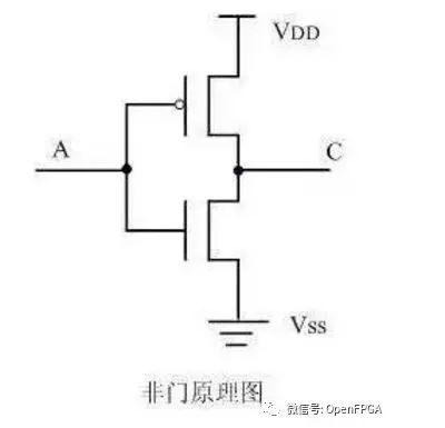
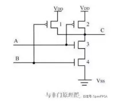
27. Basic Concepts of MOS Transistor and Drawing:
MOS (Metal-Oxide-Semiconductor) transistor consists of gate (G), drain (D), and source (S). There are two types: PMOS and NMOS, differentiated by the fact that when the gate level is high, the N-type transistor conducts, and the P-type transistor is off. They often appear in pairs, known as CMOS. As long as one conducts, the other is off. Modern microcontrollers are mainly made using CMOS technology. Drawing typically requires a simple logic expression to illustrate the CMOS circuit structure. It is necessary to master the implementation methods of commonly used logic gates.
46 Basic Questions About FPGA You Should Know
Overall, it is quite memorable that both NAND and NOR gates consist of two MOS transistors each, with the upper being PMOS and the lower being NMOS. The difference lies in the fact that NAND is “upper parallel and lower series” while NOR is “upper series and lower parallel.”
28. Detailed FPGA Design Process (Interview Questions)
Similar to the digital IC design process, taking Xilinx Vivado tools as an example, the main steps are: system planning, RTL input, behavioral simulation, logic synthesis, post-synthesis simulation (optional), post-synthesis design analysis (timing and resources), design implementation (including layout and routing optimization), post-implementation design analysis (timing and resources), board-level debugging, and bitstream solidification.
29. What Timing Paths Are Related to Timing Constraints?

Input paths: External pins to internal registers.

Register-to-register paths: Internal register to register paths.

Output paths: Internal registers to external pins.

Port to port paths: FPGA input port to output port paths (not commonly used).

30. Key Steps in Creating Timing Constraints:

Baseline constraints: create clocks, define clock interactions.

I/O constraints: set input and output delays.

Exception constraints: set timing exceptions (set_max_delay/set_min_delay, set_multicycle_path, set_false_path).

Initially, I/O constraints can be omitted, but baseline constraints should be established as early as possible.

31. Differences Between SRAM and DRAM:
SRAM is static random-access memory, storing data with transistors, requiring no refresh, and has fast read/write speeds.
DRAM is dynamic random-access memory, storing data with capacitors, requiring dynamic refresh due to capacitor leakage, and has slower read/write speeds than SRAM but lower costs, suitable for large-capacity external caching.
32. What Are the Differences Between CMOS and TTL Circuits?
The differences mainly lie in three aspects:
Structure: CMOS circuits are made of field-effect transistors, while TTL is made of bipolar transistors.
Voltage Range: CMOS logic has a larger voltage range (5~15V), while TTL operates below 5V, so CMOS has greater noise tolerance and stronger anti-interference ability.
Power Consumption and Speed: CMOS consumes less power than TTL but has a lower operating frequency.
TTL cannot directly drive CMOS levels without a pull-up resistor, while CMOS can directly drive TTL.
33. JTAG Interface Signals and Functions:
JTAG actually uses only four signals: Clock TCK, State Machine Control Signal TMS, Data Input Signal TDI, and Data Output Signal TDO.
34. Uses of Pull-Up Resistors:

1. When a TTL circuit drives a CMOS circuit, if the high level output from the TTL circuit is below the minimum high level of the CMOS circuit (generally 3.5V), a pull-up resistor is needed at the TTL output to increase the output high level value.

2. OC gate circuits must have pull-up resistors to increase the output high level value.

3. To increase the driving capability of output pins, some microcontroller pins often use pull-up resistors.

4. In CMOS chips, to prevent damage from static electricity, unused pins should not be left floating; they are usually connected to pull-up resistors to lower input impedance and provide a discharge path.

5. Adding pull-up resistors to chip pins increases output levels, thus enhancing noise tolerance and anti-interference ability.

6. Increases the bus’s resistance to electromagnetic interference. Floating pins are more susceptible to external electromagnetic interference.

7. In long line transmission, impedance mismatch can easily cause reflection wave interference; adding pull-up resistors matches impedance, effectively suppressing reflection wave interference.

35. There Are Four Multiplexing Methods, Write Out the Other Three Besides Frequency Division Multiplexing:
Four multiplexing methods: Frequency Division Multiplexing (FDMA), Time Division Multiplexing (TDMA), Code Division Multiplexing (CDMA), and Wavelength Division Multiplexing (WDM).
36. What Is Kirchhoff’s Theorem?
Kirchhoff’s laws include the current law and the voltage law:
Current Law: In a lumped circuit, at any given moment, the sum of currents flowing into a node equals the sum of currents flowing out of that node.
Voltage Law: In a lumped circuit, at any given moment, the sum of electromotive forces around any closed loop equals the sum of voltage drops across the resistors in that loop.
37. Three-Stage State Machine:
One-stage: Only one always block, implementing all logic (inputs, outputs, states) in a single always block’s sequential logic. This approach appears concise but is not maintainable; if the state is complex, it is easy to make mistakes and is not recommended. It can be used in simple state machines.
Two-stage: There are two always blocks, separating sequential logic and combinational logic. The sequential logic handles the transition between the current state and the next state, while the combinational logic implements inputs, outputs, and state judgments. This approach not only facilitates reading, understanding, and maintenance but also aids the synthesizer in optimizing code and allows users to add suitable timing constraints, benefiting layout and routing. In two-stage descriptions, the output of the current state is implemented using combinational logic, which may lead to races and hazards, producing glitches.
It is required that the outputs of the state machine be registered with a clock pulse, but in many cases, inserting a registered pulse is not allowed. In such cases, a three-stage description is used. Its advantage is that it can determine the current state’s output based on the state transition rules from the previous state according to input conditions, thus eliminating the need to insert extra clock pulses.
Three-stage: There are three always blocks, one for sequential logic describing state transitions using synchronous timing, one for combinational logic determining state transition conditions and describing state transition rules, and the third module using synchronous timing to describe the output of each state. The code is easier to maintain, and the output of the sequential logic solves the glitches from the combinational logic in the two-stage approach, but from a resource consumption perspective, the three-stage approach consumes more resources. The main difference between the two-stage and three-stage methods is whether the output of each state is implemented using combinational logic or sequential logic; combinational logic may lead to races and hazards, producing glitches.
38. What Is a State Diagram?
A state diagram describes the state transition rules of a sequential logic circuit and the relationship between outputs and inputs using geometric shapes.
39. Design a 7-bit Presettable Counter Using a Design Method You Are Familiar With, What About 15-bit?
module counter7(clk, rst, load, data, cout);
input clk, rst, load;
input [2:0] data;
output reg [2:0] cout;
always@(posedge clk) begin
if(!rst)
cout <= 3’d0;
else if(load)
cout <= data;
else if(cout >= 3’d6)
cout <= 3’d0;
else
cout <= cout + 3’d1;
end
endmodule
40. What Programmable Logic Devices Do You Know?
PAL, PLA, GAL, CPLD, FPGA.
41. Differences Between SRAM, FLASH MEMORY, DRAM, SSRAM, and SDRAM?

SRAM: Static Random Access Memory, fast access speed, but small capacity, data is lost after power off, unlike DRAM which requires constant REFRESH, and has higher manufacturing costs, usually used as cache memory.

FLASH: Flash memory, slower access speed, large capacity, data is retained after power off.
DRAM: Dynamic Random Access Memory, must constantly refresh the voltage difference, otherwise the voltage difference will drop to insufficient energy to represent the state of each memory unit. It is cheaper than SRAM but has slower access speeds and higher power consumption, commonly used as computer memory.
SSRAM: Synchronous Static Random Access Memory. All accesses to SSRAM are initiated on the rising/falling edge of the clock. Address, data input, and other control signals are all related to the clock signal.
SDRAM: Synchronous Dynamic Random Access Memory.
42. Differences Between Active and Passive Filters:
Passive filters: These circuits mainly consist of passive components R, L, and C.
Active filters: Composed of integrated operational amplifiers and R, C, they have advantages such as no need for inductors, small size, and lightweight. The open-loop voltage gain and input impedance of integrated operational amplifiers are both high, and they have a small output impedance, providing voltage amplification and buffering when forming active filter circuits. However, the bandwidth of integrated operational amplifiers is limited, making it difficult for current active filter circuits to operate at high frequencies.
43. What Are Synchronous Logic and Asynchronous Logic?

Synchronous sequential logic circuits have the characteristic that all flip-flops’ clock terminals are connected together and to the system clock terminal; the circuit’s state can only change when the clock pulse arrives. The changed state will remain until the next clock pulse arrives, making every state in the state table stable regardless of external input changes.
Asynchronous sequential logic circuits can use clocked flip-flops as well as flip-flops and delay elements without clocks as storage elements, with no unified clock in the circuit; changes in circuit states are directly caused by changes in external inputs. Synchronous logic has a fixed causal relationship between clocks, while asynchronous logic does not.
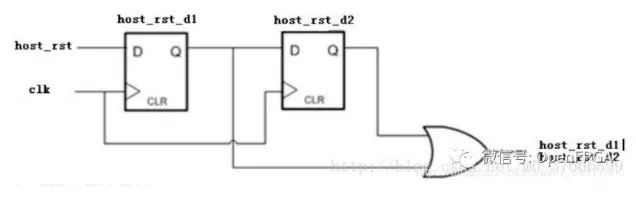
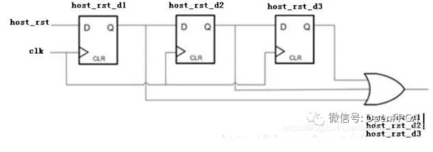
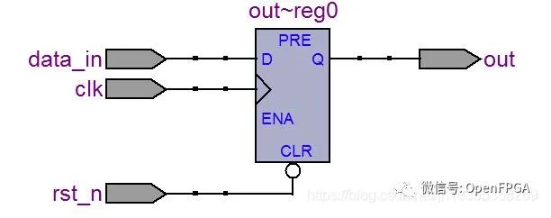
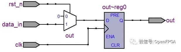
44. Differences Between Synchronous Reset and Asynchronous Reset:

Synchronous reset is performed when the clock edge changes.
Advantages: 1) High anti-interference ability, can filter out glitches in the reset signal with periods shorter than the clock period; 2) Beneficial for static timing analysis tools; 3) Beneficial for clock-based simulation tools.
Disadvantages: 1) Occupies more resources; 2) Requires the pulse width of the reset signal to exceed the clock period due to line delays; it may require multiple clock cycles of reset pulse width, and it is difficult to ensure the timing of the reset signal reaches each register; 3) Synchronous reset depends on the clock; if there are issues with the clock signal in the circuit, it cannot reset.
Asynchronous reset completes the reset action as long as the reset signal meets the conditions.
Advantages: 1) Does not require additional logic resources, simple implementation; 2) The reset signal is independent of the clock.
Disadvantages: 1) The reset signal is easily affected by external interference and sensitive to glitches in the circuit; 2) The randomness of the reset signal may lead to timing violations, meaning that when the reset signal is released near the clock valid edge, it can put the circuit into a metastable state.
45. What Two Types of Storage Resources Are Available in FPGA Chips?
FPGA chips have two types of storage resources: one called block RAM, and the other is internal memory configured by LUT (distributed RAM). Block RAM consists of a certain number of fixed-size storage blocks, and using BLOCK RAM resources does not occupy additional logic resources and is fast. However, when using it, the consumption of BLOCK RAM resources is an integer multiple of its block size.
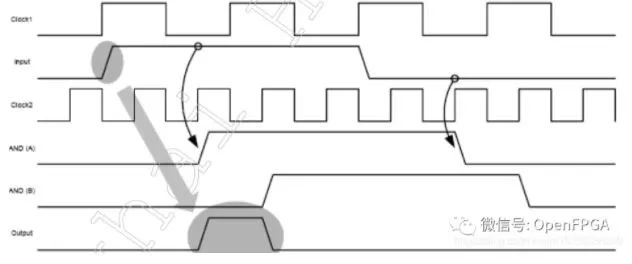
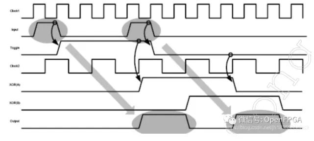
46. What Are Race and Hazard Phenomena? How to Judge? How to Eliminate?
Race: In combinational logic, when the input signal paths to the gate have different delays, resulting in inconsistent arrival times at that gate, it is called a race condition.
Hazard: The instantaneous error caused by a race condition is called a hazard (the glitches caused by races are called hazards).
Judgment methods: 1) Algebraic method: If there are opposing signals in the Boolean expression, it is likely to produce race and hazard phenomena; 2) Graphical method: If there are two tangent Karnaugh maps and the tangential point is not surrounded by other Karnaugh maps, there is a possibility of race and hazard phenomena; 3) Experimental method: Using an oscilloscope for observation.
Solutions: 1) Add filtering circuits to eliminate glitch effects; 2) Add selective signals to avoid glitches; 3) Add or reduce redundant terms to eliminate logical hazards.
Source | OpenFPGA
46 Basic Questions About FPGA You Should Know
☞ Business Cooperation: ☏ Please call 010-82306118 / ✐ Or send an email to [email protected]
46 Basic Questions About FPGA You Should Know

Click here to read the original text, directly to Electronic Technology Application Official Website

Leave a Comment