According to reports from MEMS Consulting, recently, the research team led by Hu Gongwei from the Hubei Provincial Weak Magnetic Detection Engineering Technology Research Center at the Three Gorges University collaborated with the team of Academician Huang Wei from Northwestern Polytechnical University, and published significant research findings in the prestigious journal Nano Energy. They proposed a novel strain sensor based on a Metal-Insulator-Semiconductor (MIS) structure. This sensor cleverly couples the piezoelectric effect with the quantum tunneling effect, achieving a stable and adjustable ultra-high sensitivity across a wide bias voltage range, with a maximum sensitivity of 1.8×10⁷ and an adjustable sensitivity range exceeding 3.6×10⁵. Both key indicators far exceed those of current mainstream strain sensors, opening new pathways for high-precision tactile sensing applications in fields such as robotics, human-computer interaction, and flexible wearable devices.
As a core device that converts mechanical deformation into electrical signals, the sensitivity of strain sensors (which measures the ability to detect minute deformations) and the balance with the measurement range (to adapt to large deformation scenarios) has always been a challenge in the industry: traditional high-sensitivity sensors are often limited to narrow strain ranges, while wide-range strain sensors need to sacrifice detection accuracy. For example, resistive strain gauges have low sensitivity and struggle to capture minute physiological signals such as pulse and breath; some high-sensitivity piezoelectric strain sensors can detect slight deformations but are prone to signal overload in large deformation scenarios such as joint movements and collisions due to their fixed sensitivity.
To address this challenge, the research team innovatively proposed the core idea of “controlling the surface state of the semiconductor through bias voltage to achieve sensitivity switching.” In the piezoelectric electronic tunneling transistor of the MIS structure, the surface carriers of the semiconductor can exist in two stable states: depletion and accumulation. Under low bias voltage, the surface carriers of the semiconductor are depleted, resulting in a weak shielding effect, allowing the strain-induced piezoelectric polarization charge to modulate both the height and width of the interface barrier simultaneously and in the same direction, inducing a cascading exponential response of the tunneling current, thus putting the sensor into an ultra-high sensitivity mode capable of accurately capturing minute strains. Under high bias voltage, a large number of carriers begin to accumulate on the semiconductor surface, effectively shielding the piezoelectric polarization charge, significantly suppressing the control of the barrier, and switching the sensor to a low sensitivity mode, which can stably adapt to larger strain detection.
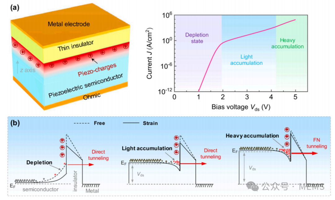
Figure 1: The impact of the piezoelectric effect on tunneling transport under different surface states in a ZnO-based Metal-Insulator-Semiconductor (MIS) piezoelectric tunneling junction (PTJ). (a) Device structure (left) and the current-voltage characteristics of three surface states (right). (b) Tunneling transport under different surface states: direct tunneling in the depletion state (left), direct tunneling in the lightly accumulated state (middle), and FN tunneling in the heavily accumulated state (right). The energy band diagrams show the cases of no strain (dashed line) and with strain (solid line).
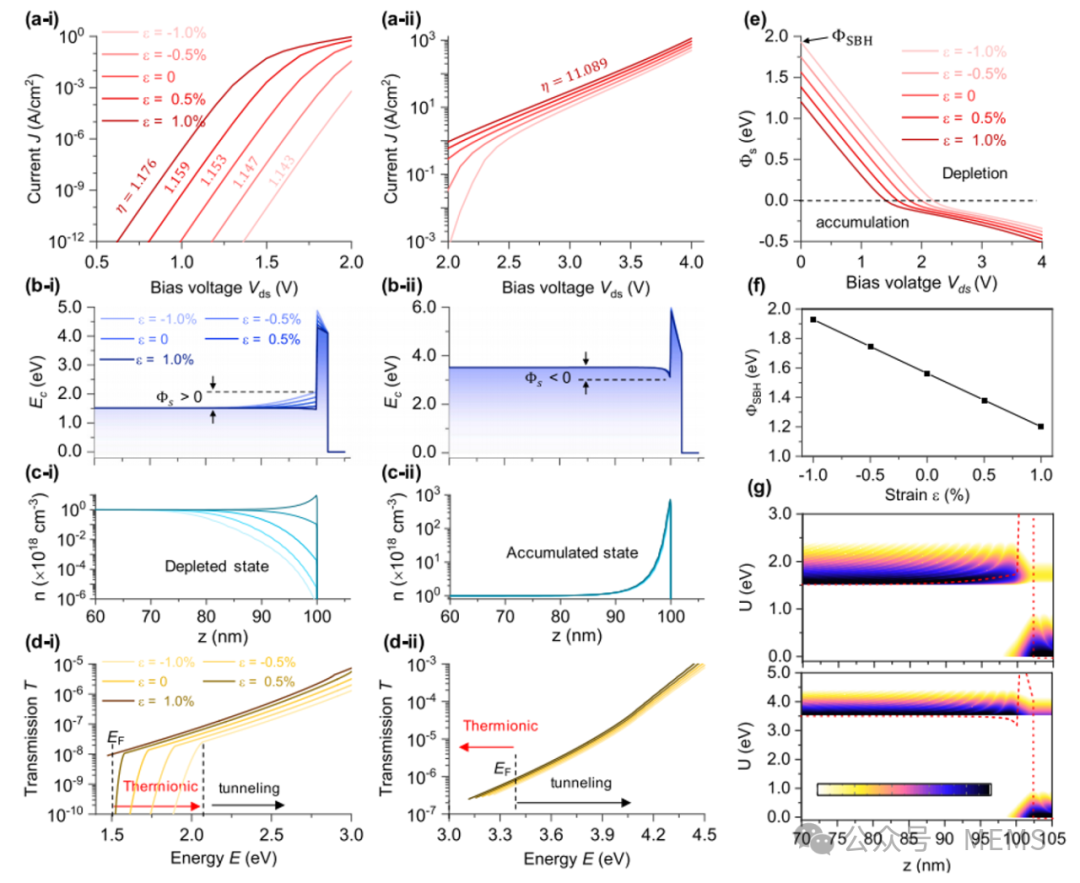
Figure 2: Piezoelectric modulation of tunneling transport in depletion and accumulation states. (a) Current-voltage characteristic curves; (b) energy band diagrams; (c) electron concentration distribution; (d) tunneling coefficients. In (b)-(d), the bias voltages are fixed at (i) Vds = 1.5 V and (ii) Vds = 3.5 V. (e) The relationship between surface potential (Φs) and strain; (f) The relationship between Schottky barrier height (ΦSBH) and bias voltage; (g) Local density of states under no strain conditions at Vds = 1.5 V (top) and 3.5 V (bottom).
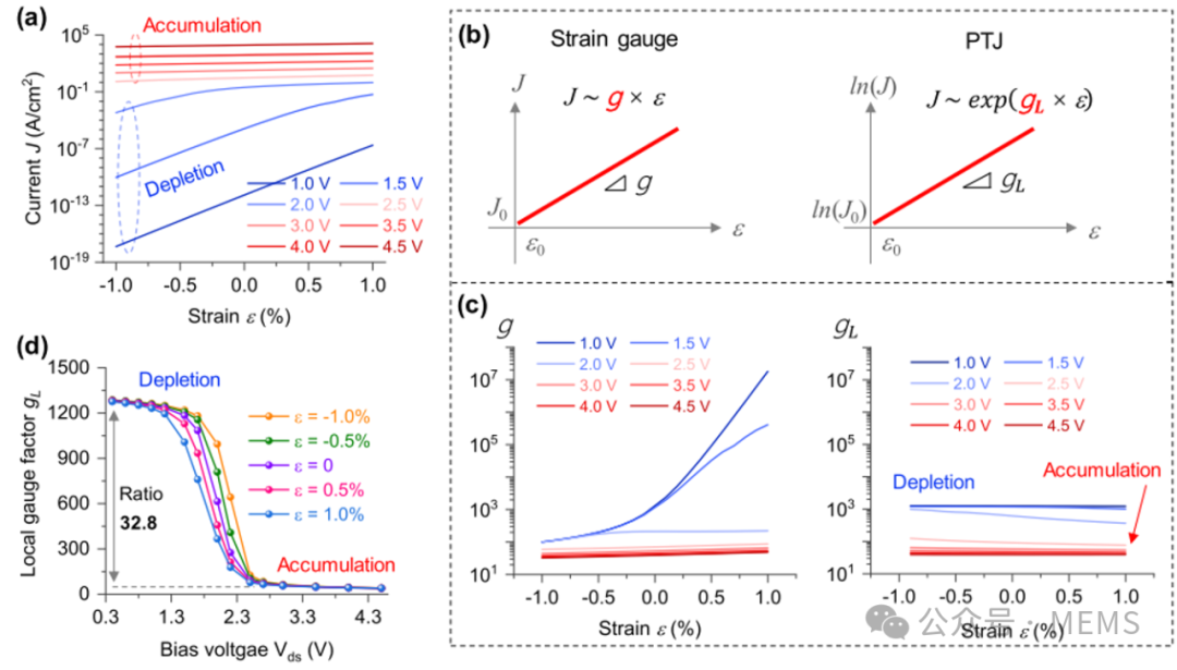
Figure 3: Local strain coefficients under piezoelectric modulation in the MIS piezoelectric tunneling junction (PJT). (a) Current-strain characteristic curves at different bias voltages; (b) Comparison of sensitivity definitions under strain-controlled linear current modulation (strain gauge, left) and exponential current modulation (piezoelectric tunneling junction, right); (c) The relationship between strain coefficient (GF, left) and local strain coefficient (right) with strain; (d) The variation of local strain coefficient with bias voltage under different strains.
The switching between the above two states can be achieved simply by adjusting the external bias voltage, without changing the physical structure of the device, allowing for fast and reversible responses, thus achieving high sensitivity and wide range detection in strain sensors. Additionally, the team systematically studied the effects of key parameters such as insulator thickness, doping concentration, and material selection, further optimizing the device’s performance.
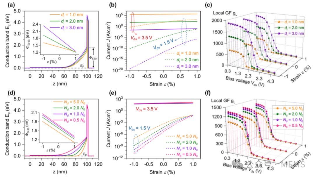
Figure 4: The impact of insulator thickness and doping concentration on the sensing performance of the piezoelectric tunneling junction (PJT). (a, d) Energy band diagrams and strain-related Schottky barrier heights (insets) under equilibrium states; (b, e) The relationship between current and strain under low bias (1.5 V) and high bias (3.5 V); (c, f) The relationship of local strain coefficient (local GF) with bias voltage and strain. In (a)-(c), the structural parameters used are: insulator thickness (di) of 1.0 nm, 2.0 nm, and 3.0 nm, with doping concentration (Nd) fixed at N0; in (d)-(f), the structural parameters used are: doping concentrations (Nd) of 0.5N0, 1.0 N0, 2.0 N0, and 5.0 N0 (N0 = 1.0×10¹⁸ cm⁻³), with insulator thickness (di) fixed at 2.0 nm.
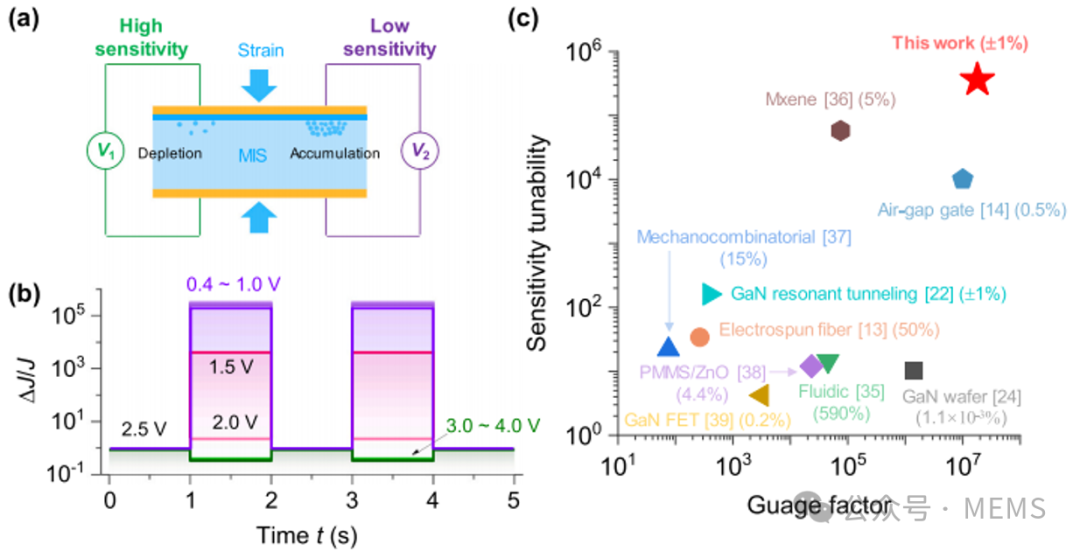
Figure 5: The impact of insulator materials and metal electrodes on the sensing performance of the piezoelectric tunneling junction (PJT). (a, d) Energy band diagrams and strain-related Schottky barrier heights (insets); (b, e) The relationship between current and strain under low bias (1.5 V) and high bias (3.5 V); (c, f) The relationship of local strain coefficient (local GF) with bias voltage and strain. In (a)-(c), the metal electrodes used are gold (Au), and the insulator materials are hafnium dioxide (HfO₂), zirconium dioxide (ZrO₂), and aluminum oxide (Al₂O₃); in (d)-(f), the insulator material is aluminum oxide (Al₂O₃), and the metal electrodes are aluminum (Al), nickel (Ni), and gold (Au). In this figure, the insulator thickness is fixed at di= 2.0 nm, and the doping concentration is fixed at N0 = 1.0×10¹⁸ cm⁻³.
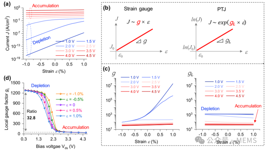
Figure 6: Adjustable sensitivity characteristics and performance comparison of the piezoelectric tunneling junction (PJT). (a) Device structure of the adjustable sensitivity strain sensor: high sensitivity at bias voltage V₁ (depletion state) and low sensitivity at bias voltage V₂ (accumulation state); (b) The relative change in current (ΔJ/J) controlled by bias voltage over time; (c) Comparison of sensitivity (gauge factor) and adjustable range among various strain sensors. Note: Both sensing modes (high sensitivity and low sensitivity) are achieved on the same device structure, and can be switched simply by adjusting the external bias voltage without physical reconstruction.
Paper link:
https://doi.org/10.1016/j.nanoen.2025.111440