| Based on semiconductor technology, the CCD image sensor has changed the history of how humans record images with film. Today, digital imaging is not only an important tool for scientific analysis but has also deeply integrated into everyone’s daily life. |

Willard S. Boyle (left) and George E. Smith (right) invented CCD technology in 1969. Source: Literature [1]
In 2009, Willard S. Boyle and George E. Smith were awarded the Nobel Prize in Physics for their invention of the CCD (Charge-Coupled Device), also known as the CCD image sensor.
Joseph Nordgren, chairman of the Nobel Prize Committee, stated during the announcement of the award: “The way we record images in today’s society is entirely based on the research of CCD. The practical significance of this research is enormous… it has changed our lives, not only in the scientific field but across society as a whole.”
Film Era
Before the invention of the digital camera in 1975, people recorded images using film. The process can be summarized as follows: light passes through the camera lens, and the shutter speed determines the amount of exposure. The light causes a chemical reaction in the silver salts on the film, ultimately generating a latent image on the film. The image is then developed in a darkroom to create a negative, which is finally printed using a developer.
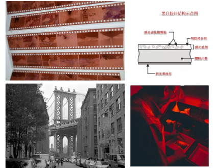
Film photography requires complex processing to obtain an image.
[Image source from the internet]
Invention of CCD
In October 1969, Smith and Boyle had a discussion over lunch at Bell Labs that sparked the idea for CCD. They continued to explore the concept after lunch and came up with the idea for this ubiquitous imaging invention on that very day. However, the journey from creating a prototype to developing a practical technology usable by scientists and photographers was long and arduous. Although CCD later dominated the field of astronomy, its initial resolution was very low and not practical for use. At that time, the signal-to-noise ratio of CCD was poor, making it difficult to foresee its bright future.
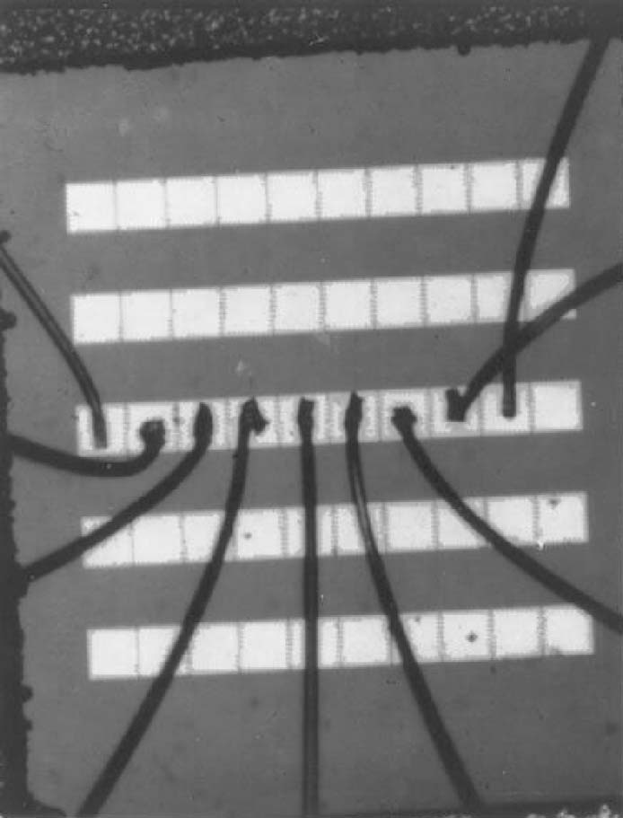
The first CCD device
Source: Literature [4]
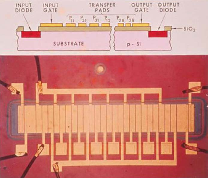
The first CCD integrated device
Source: Literature [4]
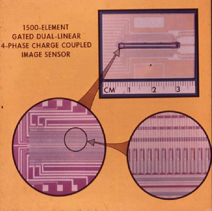 Early linear imaging CCDSource: Literature [4]
In the following years, hundreds of scientists and engineers worked tirelessly to gradually push CCD towards practicality. Companies like Fairchild, Tektronix, and Texas Instruments in the U.S., as well as Sharp, Sony, Toshiba, and NEC in Japan, made numerous contributions. Applications in aerospace, science, and consumer fields benefited from funding invested from various channels to solve CCD issues; however, the challenges remained tough, and it was a very arduous development path.
Principle of CCD
CCD is a type of semiconductor device that can convert optical images into digital signals. The tiny light-sensitive materials embedded on the CCD are called pixels. The higher the number of pixels and the larger the area, the higher and clearer the imaging quality. The CCD has many neatly arranged capacitors that can sense light, store signals, and convert images into digital signals. Controlled by external circuitry, each small capacitor can transfer its charge to the adjacent image processor to form an image.MOS capacitors are the most basic unit that makes up the CCD, being the simplest structure in the metal-oxide-semiconductor (MOS) device.
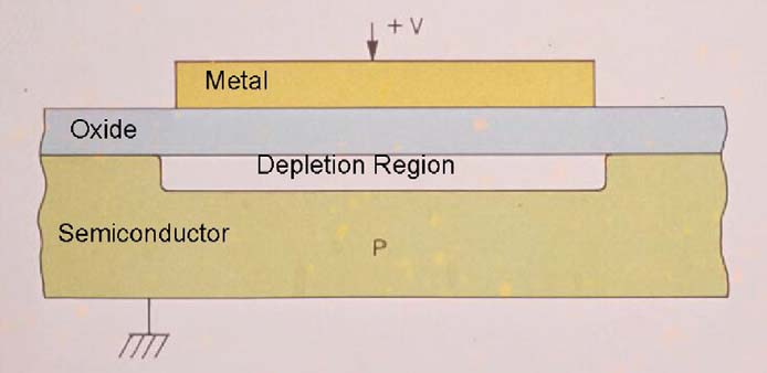
MOS capacitorSource: Literature [4]The basic working process of CCD mainly involves the generation, storage, transfer, and detection of signal charges:(1) Signal charge injection (generation): In CCD, the method of charge injection can be divided into two categories: optical injection and electrical injection. When light strikes the CCD silicon wafer, electron-hole pairs are generated in the semiconductor near the gate. Most carriers are repelled by the gate voltage, while a few carriers are collected in the potential well to form signal charges.
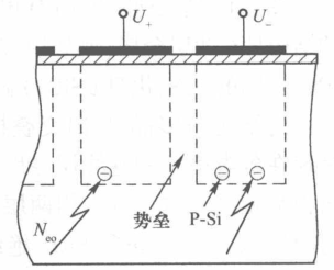
Back-illuminated optical injectionSource: Literature [8]Electrical injection means that the CCD samples the signal voltage or current through the input structure, and then converts the signal voltage or current into signal charge injected into the corresponding potential well. Common methods of electrical injection include current injection and voltage injection.
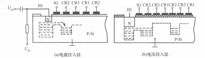
Electrical injection method
Source: Literature [8]
(2) Signal charge storage: The second step of the CCD working process is the collection of signal charges, which is the process of collecting the charges excited by incident photons into signal charge packets.
When a positive bias is applied to the electrode on the SiO2 surface, a depletion region (potential well) is formed in the P-type silicon substrate, and the depth of the depletion region increases with the positive bias. The minority carriers (electrons) are absorbed into the region under the highest positive bias electrode, forming charge packets (potential wells). For N-type silicon substrate CCD devices, the minority carriers are holes when a positive bias is applied to the electrode.
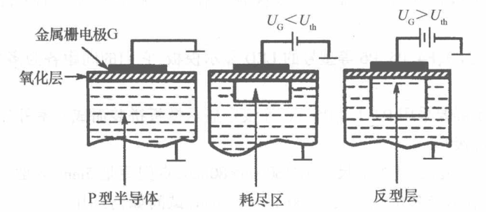
Charge storage
Source: Literature [8]
(3) Signal charge transfer (coupling): The third step of the CCD working process is the transfer of signal charge packets, which is the process of transferring the collected charge packets from one pixel to the next until all charge packets are output.
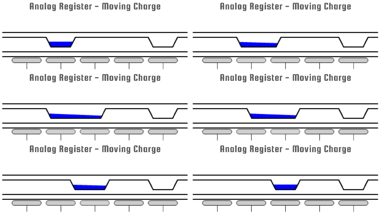
Charge transfer
Source: Literature [7]
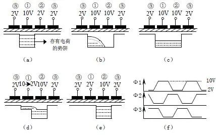
Charge transfer methods in three-phase CCD
(a) Initial state; (b) Charge transfers from electrode ① to electrode ②; (c) Charge is evenly distributed under electrodes ① and ②; (d) Charge continues to transfer from electrode ① to electrode ②; (e) Charge is completely transferred to electrode ②; (f) Three-phase overlapping pulse.
Source: Literature [8]
(4) Signal charge detection: The fourth step of the CCD working process is the detection of charges, which is the process of converting the charges transferred to the output stage into current or voltage.The types of charge output mainly include three types: 1) current output; 2) floating gate amplifier output; 3) floating diffusion amplifier output.
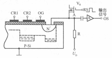
Charge detection circuit
Source: Literature [8]
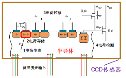
Schematic diagram of the CCD working process
Source: Literature [6]
The CCD image sensor is an array composed of MOS (metal-oxide-semiconductor) capacitors arranged in a specific pattern. A very thin layer (about 120nm) of silicon dioxide is grown on a P-type or N-type silicon substrate, and then metal or doped polysilicon electrodes (gates) are deposited sequentially on the silicon dioxide layer, forming a regular array of MOS capacitors. With the addition of input and output diodes at both ends, the CCD chip is constructed.According to the different arrangements of pixels, CCDs can be divided into two main categories: linear arrays and area arrays.Linear array CCDs scan one line at a time; to obtain the video signal of the entire two-dimensional image, scanning methods must be employed. Linear array CCDs are further divided into single-channel and dual-channel linear array CCDs.Single-channel linear array CCD: More transfer times with lower efficiency, suitable only for imaging devices with fewer pixel units.Dual-channel linear array CCD: Reduces the transfer times by half, thereby improving its total transfer efficiency to double that of the original.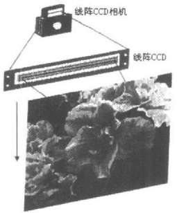
Linear array CCD
Source: Literature [6]
Area array CCD: A two-dimensional array can be formed by arranging the one-dimensional linear array CCD’s light-sensitive units and shift registers in a specific manner. The area array CCD exposes the entire image simultaneously.Frame transfer area array CCD—Advantages: Simple electrode structure, small photosensitive area. Disadvantages: Requires a larger temporary storage area.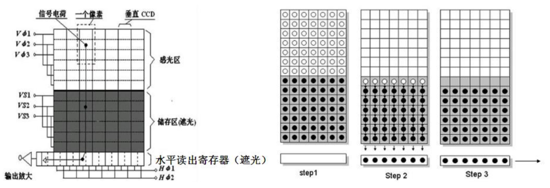 Frame transfer area array CCD structure and working process
Source: Literature [6]
Interline transfer area array CCD—Advantages: Significantly improved transfer efficiency. Disadvantages: More complex structure.
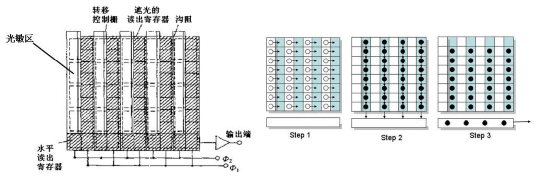
Interline transfer area array CCD structure and working process
Source: Literature [6]
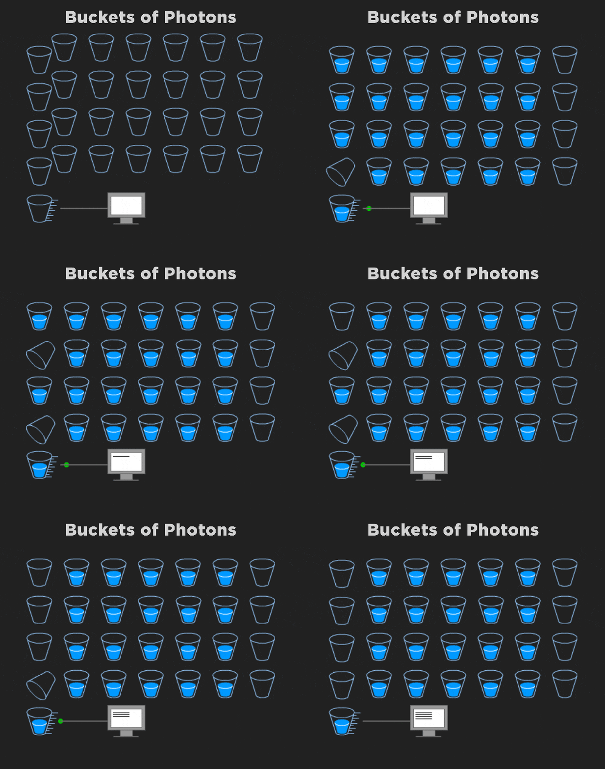 CCD function schematicSource: Literature [7]
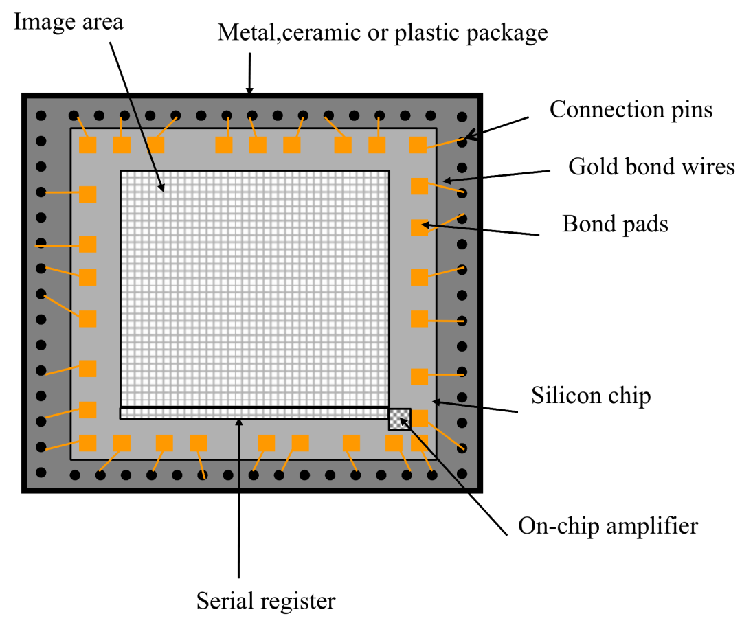
CCD chip structure
Image source from the internet
Development of CCD
The invention of CCD is of epoch-making significance, greatly extending and enhancing the ability of humans to capture information through the important organ of vision, accounting for 85% of our sensory input.Three main factors have facilitated the rapid development of CCD: First, CCDs are small in size, lightweight, consume less power, have ultra-low noise, a large dynamic range, good linearity, reliability, and durability. Second, these devices can compete with vacuum tubes in terms of shape, speed, form quality, and cost. Third, new detectors are needed for space imaging applications.In the 1970s, Bell Labs in the U.S. successfully developed the world’s first CCD, which led to a leap in imaging and video technology.In 1973, Fairchild began applying CCD technology in commercial fields, producing the first commercial CCD imaging device, paving the way for CCD in industrial applications.By the late 1980s, CCD had replaced electronic tubes in most video applications.Entering the 1990s, CCD was used for resolution imaging, widely applied in professional electronic photography, space exploration, X-ray imaging, and other scientific fields.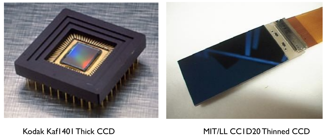
Two types of CCD products
Image source from the internet
The results of market applications prove that CCD is a significant technological revolution in the scientific field. After being overlooked for decades, it rightfully received the Nobel Prize in 2009.
Continuous Transformation
However, the progress of science and technology has never stopped.In 1998, CMOS image sensors (Complementary Metal-Oxide-Semiconductor Image Sensor, CIS) were born.The photoelectric information conversion function of CMOS is fundamentally similar to that of CCD, with the difference being in how the information is transmitted after photoelectric conversion.CMOS features simple reading methods, fast output rates, low power consumption (about 1/10th of that of CCD chips), small size, lightweight, high integration, and low cost.Since 2008, major manufacturers have gradually begun using back-illuminated CMOS in various digital camera products.Since then, CMOS image sensors have rapidly developed.
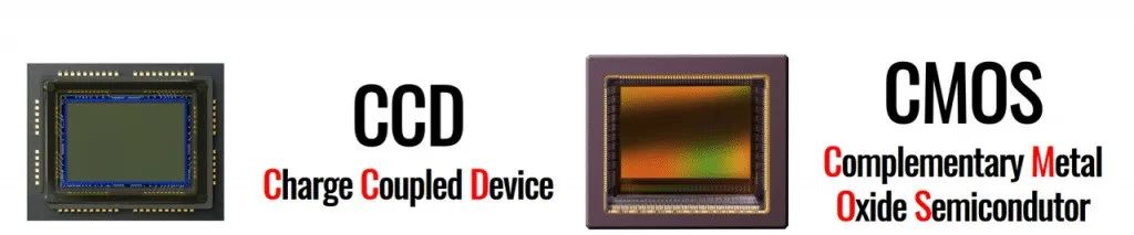
CMOS replaces CCD
Image source from the internet
As technology continues to evolve, we believe that in the future, more types of sensors will emerge. This is just a matter of time. When we look back at the past, reflecting on the film era, the CCD era, and the CMOS era, we will surely marvel at the rapid advancements in technology.
References
-
https://www.nobelprize.org/prizes/physics/2009/summary/
-
Zhang Rujing. The Story Behind the Semiconductor Industry[M]. Tsinghua University Press, 2013.
-
Dong Yiting. Research on the Development of Photography Technology and Its Role in Contemporary Society[D]. Harbin Normal University, 2016.
-
Smith, G. E. (2009). “The invention and early history of the CCD.” Nuclear Instruments and Methods in Physics Research Section A: Accelerators, Spectrometers, Detectors and Associated Equipment 607(1): 1-6.
-
https://www.microscopyu.com/digital-imaging/introduction-to-charge-coupled-devices-ccds
-
https://www.mega-9.com/tech/tech-45.html
-
https://specinstcameras.com/what-is-a-ccd/
-
Wang Qingyou. Application Technology of Image Sensors[M]. Electronics Industry Press, 2019.
-
https://www.docin.com/p-505990925.html
-
http://dc.yesky.com/88/31913588all.shtml
Copyright Notice: Any form of media reproduction and excerpting without authorization is strictly prohibited, and reproduction to platforms other than WeChat is forbidden!
Editor: Shuyu