Hello everyone, I am Pi Zi Heng, a serious techie. Today I will introduce the precautions for configuring multiple registers of serial NOR Flash in FDCB.
Regarding the use of the i.MXRT boot header FDCB to set the internal registers of Flash, I have previously written two articles. Before diving into this article, I recommend reading these two articles for a preliminary understanding.
“Setting Dummy Cycle for Flash in FDCB” “Switching Flash Mode to QPI/OPI in FDCB”
We know that Flash often has multiple state/configuration registers, some of which are volatile and some are non-volatile. When the chip is designated to boot from Flash, if we want the BootROM to pre-configure these Flash registers according to different application requirements, then there is no need for additional configuration in the application program (involving configuration changes in Flash working state, if it is an XIP program, code redirection issues need to be considered).
For configuring a register of Flash using FDCB, I believe everyone is familiar with it, as there are successful examples by default in the NXP SDK package. Recently, a colleague of mine tried to use FDCB to configure two registers of Micron MT35X (the register at address 0x000000 to switch to OPI DDR, and the register at address 0x000003 to set Drive Strength) and found that one of the register settings did not take effect. What is going on? Today we will discuss this:
Note: This article is applicable to i.MXRT500/600/1010/1020/1040/1050/1060/1160/1170
1. Flash Register Configuration Capabilities Provided by FDCB
First, let’s take a look at the members related to Flash configuration in the FDCB structure, which I have organized as follows. In simple terms, there is a deviceModeSeq and three configCmdSeqs, so a maximum of four different commands can be configured for corresponding registers in Flash (some Flash configurations can write multiple registers in a single command, allowing for more than four registers to be configured), which is sufficient for most application scenarios.
Note 1: The order of execution for these four configurations by BootROM is deviceModeSeq, configCmdSeqs[0], configCmdSeqs[1], configCmdSeqs[2], remember this order. Note 2: The configuration functions achieved by deviceModeSeq and configCmdSeq are almost indistinguishable; they can do the same things and are interchangeable.
//!@brief FlexSPI Memory Configuration Block
typedef struct _FlexSPIConfig
{
    // ...

    //!< [0x010-0x010] Device Mode Configure enable flag, 1 - Enable, 0 - Disable
    uint8_t deviceModeCfgEnable;
    //!< [0x011-0x011] Specify the configuration command type:Quad Enable, DPI/QPI/OPI switch, Generic configuration, etc.
    uint8_t deviceModeType;
    //!< [0x012-0x013] Wait time for all configuration commands, unit: 100us
    uint16_t waitTimeCfgCommands;
    //!< [0x014-0x017] Device mode sequence info, [7:0] - LUT sequence id, [15:8] - LUt sequence number, [31:16] Reserved
    flexspi_lut_seq_t deviceModeSeq;
    //!< [0x018-0x01b] Argument/Parameter for device configuration
    uint32_t deviceModeArg;

    //!< [0x01c-0x01c] Configure command Enable Flag, 1 - Enable, 0 - Disable
    uint8_t configCmdEnable;
    //!< [0x01d-0x01f] Configure Mode Type, similar as deviceModeTpe
    uint8_t configModeType[3];
    //!< [0x020-0x02b] Sequence info for Device Configuration command, similar as deviceModeSeq
    flexspi_lut_seq_t configCmdSeqs[3];
    //!< [0x030-0x03b] Arguments/Parameters for device Configuration commands
    uint32_t configCmdArgs[3];

    // ...

    //!< [0x07c-0x07d] Busy offset, valid value: 0-31
    uint16_t busyOffset;
    //!< [0x07e-0x07f] Busy flag polarity, 0 - busy flag is 1 when flash device is busy, 1 - busy flag is 0 when flash device is busy
    uint16_t busyBitPolarity;
    //!< [0x080-0x17f] Lookup table holds Flash command sequences
    uint32_t lookupTable[64];

    // ...

} flexspi_mem_config_t;
At the end of the article “Setting Dummy Cycle for Flash in FDCB”, I have already shared the code flow of BootROM parsing and executing configCmdSeq. In this process, we can see the logical code related to the members deviceModeType/configModeType[], waitTimeCfgCommands, and it is necessary to further explain this.
//!@brief Flash Configuration Command Type
enum
{
    kDeviceConfigCmdType_Generic,    //!< Generic command, for example: configure dummy cycles, drive strength, etc
    kDeviceConfigCmdType_QuadEnable, //!< Quad Enable command
    kDeviceConfigCmdType_Spi2Xpi,    //!< Switch from SPI to DPI/QPI/OPI mode
    kDeviceConfigCmdType_Xpi2Spi,    //!< Switch from DPI/QPI/OPI to SPI mode
    kDeviceConfigCmdType_Spi2NoCmd,  //!< Switch to 0-4-4/0-8-8 mode
    kDeviceConfigCmdType_Reset,      //!< Reset device command
};
When the deviceModeType/configModeType members are set to kDeviceConfigCmdType_Spi2Xpi; if the BootROM uses DPI/QPI/OPI commands when obtaining the FDCB (determined by efuse configuration), then this Flash register configuration will be ignored; if the BootROM uses the ordinary single-line SPI mode to read the FDCB, then this Flash register configuration will still be effective.
The three configuration types related to switching Flash command modes, kDeviceConfigCmdType_Spi2Xpi, indicate that these configurations will cause changes in the Flash working mode. Once the Flash working mode changes, the READ_STATUS command used to determine whether the configuration is complete also becomes unavailable (because the command sequences in SPI mode differ from those in DPI/QPI/OPI mode), in which case we need to use the waitTimeCfgCommands member to implement software delay to wait for the Flash configuration to take effect (if we proceed to the next process without waiting for it to take effect, it may lead to boot issues).
The kDeviceConfigCmdType_Generic configuration type is used for Flash register configurations unrelated to mode switching. In this case, the BootROM can use the READ_STATUS command to determine whether the configuration of the Flash registers has taken effect, and thus there is no need to implement a delay using waitTimeCfgCommands (you need to refer to the Flash data manual for corresponding settings, which can be cumbersome, and the manual provides typical and maximum values, taking the maximum value may lead to longer boot times, while the typical value cannot guarantee applicability in all situations).
2. Precautions for Configuring Multiple Registers of Flash
The writing process for Flash configuration registers usually consists of three steps: 1. WRITE_ENABLE to enable write operations; 2. specific CONFIG_REG operations; 3. READ_STATUS or software delay to ensure that the configuration is complete. All these command sequences are stored in the lookupTable[64] member in FDCB.
Regarding the configuration operations of Flash registers, from the perspective of register attributes, they can be divided into volatile and non-volatile types. The former typically takes effect immediately, while the latter does not (the Flash status register WIP bit reflects the progress). From the command mode perspective, they can be divided into non-mode-switching operations (such as setting Dummy Cycle, Drive Strength) and operations that switch between SPI and DPI/QPI/OPI modes, with the former taking effect immediately and the latter not.
Now back to the issue my colleague encountered at the beginning of the article. If deviceModeSeq is used to switch to OPI DDR mode and configCmdSeqs[0] is used to set Drive Strength, which operation did not take effect? I won’t keep you guessing; setting Drive Strength did not take effect because the first configuration switched to OPI DDR mode, and when Flash switched to this mode, the WRITE_ENABLE command for the second/third/fourth configurations became unavailable (again because the command sequences in SPI mode differ from those in DPI/QPI/OPI mode), and thus the corresponding Flash register settings became invalid.
So how can we avoid this issue? One foolproof method is to always use configCmdSeqs[2] for switching between SPI and DPI/QPI/OPI modes, so that it will not affect the previous three configurations. As mentioned earlier, at this point, you cannot use the READ_STATUS command to determine whether the command mode switch is complete; you must use waitTimeCfgCommands for software delay. If the delay time is insufficient, and the subsequent BootROM execution reaches the verification of the IVT header while the mode switch is still incomplete, this will lead to the IVT boot header being unable to obtain it correctly, thus causing boot failure.
Assuming that the waitTimeCfgCommands delay setting is sufficient for the command mode switch, does this solve the problem? Not necessarily. If deviceModeSeq has been used to set Drive Strength, but it is necessary to write to the non-volatile memory of Flash, it is essential to ensure that the waitTimeCfgCommands delay is also sufficient for writing to the non-volatile registers. Looking at the MT35X data manual, we can find that the typical cycle time for writing to non-volatile registers is 0.2s, and the maximum value is 1s.
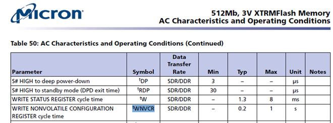
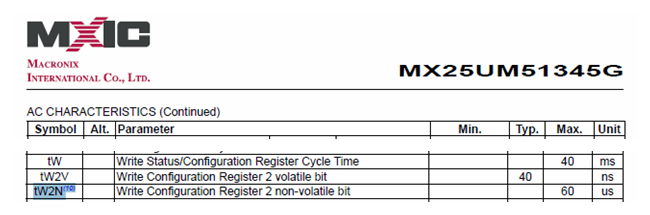
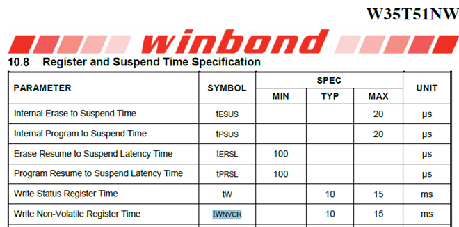
Comparing the writing times for non-volatile registers of Winbond and Macronix Octal Flash, we find that Winbond is the shortest (<=60us), Macronix is next (<=15ms), and Micron is slightly longer (<=1s). The shorter the writing time, the shorter the boot time.
If the waitTimeCfgCommands setting is insufficient for writing to the non-volatile registers, and you proceed to switch to OPI mode without waiting for the Drive Strength configuration to complete, this will cause the mode switch to fail (Flash cannot accept any write commands while busy), and of course, it cannot boot normally.
What I have introduced above are relatively complex scenarios for configuring Flash registers. If it is a simple volatile register configuration operation that does not involve mode switching, then the order of these four configurations in FDCB is not important, and there is no need to enable waitTimeCfgCommands, so there is no need to consider it too much.
With that, I have completed the introduction to the precautions for configuring multiple registers of serial NOR Flash in FDCB. Thank you for reading~

END