Dear readers, the BG (Back Grinding) process in semiconductor packaging is crucial! From film application, coarse grinding, fine grinding to polishing, each step affects the wafer thickness accuracy and warpage. Beginners often struggle with wheel selection, film material compatibility, and failure troubleshooting. This comprehensive guide, compiled from official training materials, clearly breaks down grinding equipment, core processes, material selection, and fault resolution. Whether you are a new employee or an experienced worker looking to fill knowledge gaps, save this for direct use!
1. First, understand: What exactly does the grinding process do?
The core task of Back Grinding is to reduce the wafer from its initial thickness (6-inch 625μm / 8-inch 725μm / 12-inch 775μm) to the target thickness. Its core functions are fourfold:
- Enhancing heat dissipation: Thinner wafers dissipate heat easily, preventing chip breakage due to thermal stress;
- Optimizing performance: Reducing the distance between the effective layer and the back enhances device high-frequency and electrical performance;
- Reducing package size: Adapting to the trend of “light, thin, short, and small” in electronic products;
- Facilitating subsequent processing: Laying the groundwork for cutting (WS) and die attach.
In simple terms: The quality of grinding directly determines the chip yield; one mistake can lead to the scrapping of an entire batch of wafers!
2. Core equipment: Two key models + operational workflow (must-save level)
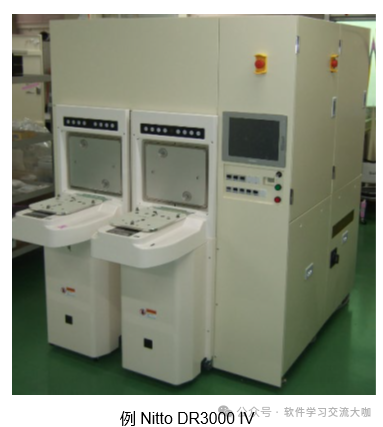
1. Film application machine: Nitto DR3000IV (key for front-end protection)
- Core function: Apply BG film on the front of the wafer to protect the passivation layer and bump (maximum compatible bump height of 200μm);
- Operational workflow: Wafer retrieval → Aligner positioning → Chuck table fixation → Automatic film application → Cutting → Return to box (fully automated with precise imaging positioning).
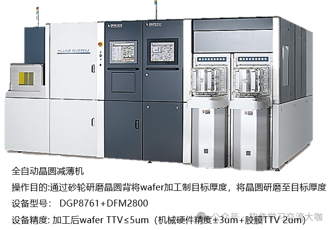
2. Integrated grinding machine: DGP8761+DFM2800 (mainstream model for 12 inches)
- Core advantage: Integrates coarse grinding, fine grinding, polishing, UV irradiation, and film application/removal, completing everything in one stop;
- Equipment precision: After processing, wafer TTV ≤ 5μm (mechanical precision ±3μm + adhesive film TTV 2μm);
- Core components: Z1 (coarse grinding spindle), Z2 (fine grinding spindle), Z3 (polishing spindle), T1/T2 handling arms;
- Operational workflow:
- Wafer retrieval → Positioning calibration;
- Z1 coarse grinding (rapid material removal) → Z2 fine grinding (precision control + damage elimination);
- Optional Z3 dry polishing (stress relief);
- Cleaning and drying → DFM2800 film application / UV irradiation → Film removal → Wafer ring material box collection.
3. Core processes: Three major stages + material selection (avoid mistakes for beginners)
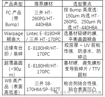
1. Film application process (Taping): Choosing the right film material is fundamental
- Film material classification: UV film (contains photosensitive agents, easy to peel off after irradiation) and non-UV film (conventional protection);
- Film material selection guide (copy directly):
2. Grinding process: Three stages + key parameters
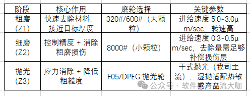
The grinding uses the “In feed rotation mode” (wafer rotation + spindle rotation), ensuring stable processing and good consistency, divided into three stages:
3. Wheel selection: Three key dimensions
The grinding wheel consists of abrasive grains, bonding agents, and voids, and the selection directly affects the grinding effect:
- Abrasive grain size: The larger the number, the smaller the particles (#320 for coarse grinding / #8000 for fine grinding). Larger numbers have higher efficiency but poorer roughness, while smaller numbers have higher precision but shorter lifespan;
- Bonding agent: Resin bonding agents (self-sharpening, suitable for fine grinding), metal bonding agents (long lifespan, suitable for glass / C/T self-grinding), ceramic bonding agents (high rigidity, suitable for coarse grinding);
- Concentration: The higher the value, the higher the proportion of abrasive grains (concentration 100 = 25% abrasive grains), the harder the wheel but with reduced heat dissipation / self-sharpening ability.
4. Common failure modes + solutions (pitfall guide)
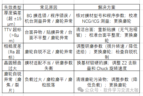
During grinding, the most common issues are thickness deviation, TTV exceeding standards, poor roughness, and warpage. Corresponding solutions are directly copied:
5. Mainstream process flows: DAG vs DBG (two core routes)
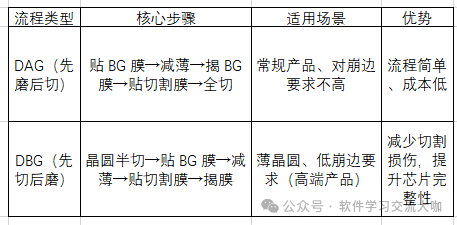
Key point: The DBG process is often paired with laser DAF processes to further separate chips, adapting to high-end packaging needs!
Interaction time
Dear readers, what has been the most troublesome issue you have encountered in the grinding process? Is it improper wheel selection leading to excessive roughness, or incorrect film material compatibility causing warpage? Share your practical pain points in the comments, and I will help you optimize solutions!
#SemiconductorGrinding #BGProcess #SemiconductorPackaging #WheelSelection #WaferThinning #BeginnerPitfalls #SemiconductorEquipment #PackagingProcess